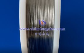
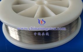
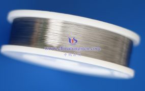
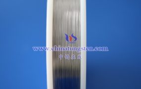
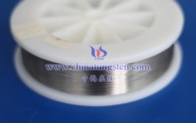
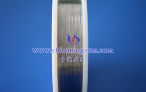
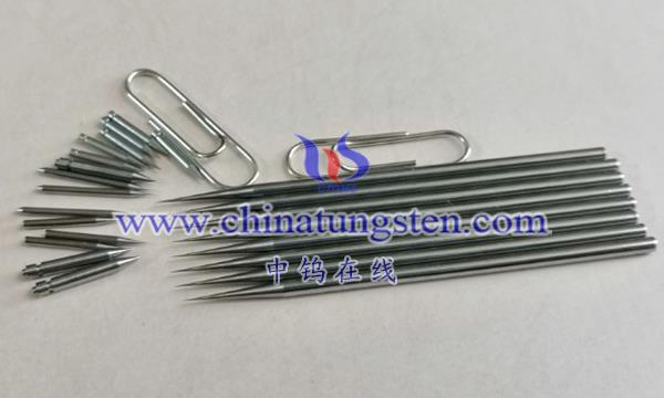
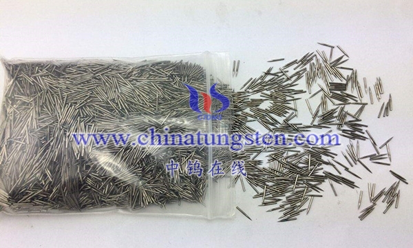
A wafer test probe is a tool used for wafer testing in semiconductor device production and is used to test integrated circuit chips on the wafer. These probes are typically tiny, precision-fabricated metal probes designed to make electrical connections to circuits on the wafer for performance and functional testing.
Here are some of the key features and capabilities of wafer test probes:
1. Tiny size: Wafer test probes are usually very small in size to enable precise electrical connections to tiny circuit components on the wafer.
2. High accuracy: These probes need to have high accuracy to ensure accurate electrical connections and measurements for reliable test results.
3. Wear resistance: Since wafer testing is a highly repetitive process, test probes need to have a certain degree of wear resistance to maintain long-term stability and performance.
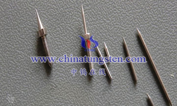
4. Electrical conductivity: Wafer test probes are usually made of metal materials with good electrical conductivity to ensure good electrical connections.
5. Automation: In high-volume semiconductor manufacturing, wafer testing often needs to be automated. Therefore, wafer test probes need to be adapted to automated systems to improve test efficiency.
6. Temperature control function: Some applications may require testing at a specific temperature, and the wafer test probe may need to have a temperature control function to ensure the stability of the test conditions.
The role of these test probes in semiconductor manufacturing is critical because they directly impact the accurate assessment of chip performance and quality. Throughout the manufacturing process, the wafer testing stage helps screen out substandard chips and ensures that the quality of the final product meets requirements.
More details of tungsten needles, please visit website: http://tungsten.com.cn/tungsten-needles-and-pins.html
Please contact CHINATUNGSTEN for inquiry and order of tungsten needles:
Email: sales@chinatungsten.com
Tel.: +86 592 5129595