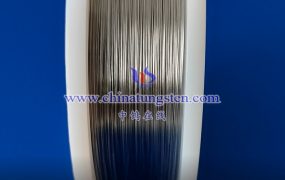
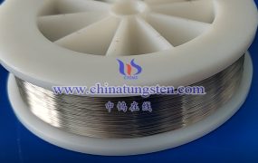
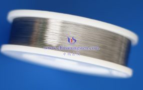
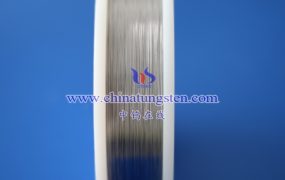
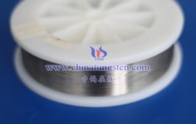
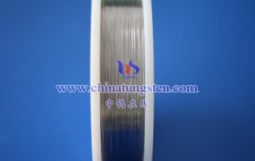
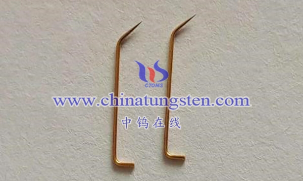
Tungsten probes for wafer scale testing typically refer to adding tiny scales or markings to the tip portion of the probe for measuring or locating specific test points. These graduations can be tiny depressions, bumps, or other shaped markings that help make precise measurements. Such designs are useful in applications that require very precise positioning or measurement.
Some features and application areas include:
1. Position positioning: The tungsten probe can be used to locate the precise position of the test point. This is important for applications that require measurements or tests at specific locations on the wafer.
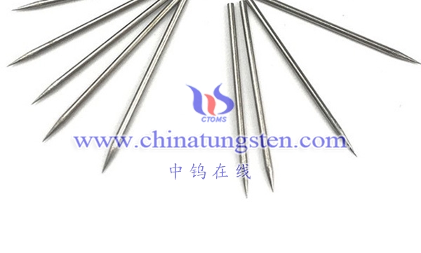
2. Measurement: Scales can be used to measure specific distances or dimensions. By observing the relative position changes between the scale and the target, precise measurements can be made.
3. Microelectronics applications: In the field of microelectronics, high-precision measurement and testing of tiny-sized circuit components is required. tungsten probes meet these requirements.
4. Laboratory Research: In scientific research or laboratory settings, graduated test tungsten probes can be used to perform microscopic scale measurements and experiments.
5. High-density testing: In high-density integrated circuits, tungsten probes can help determine and accurately measure the location and characteristics of tiny circuit components.
More details of tungsten needles, please visit website: http://tungsten.com.cn/tungsten-needles-and-pins.html
Please contact CHINATUNGSTEN for inquiry and order of tungsten needles:
Email: sales@chinatungsten.com
Tel.: +86 592 5129595