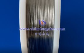
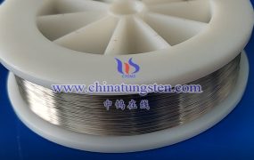
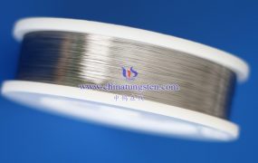
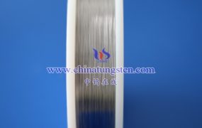
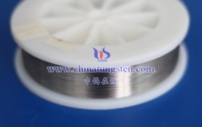
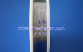
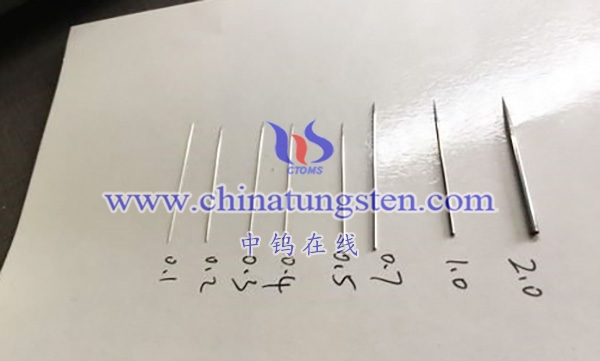
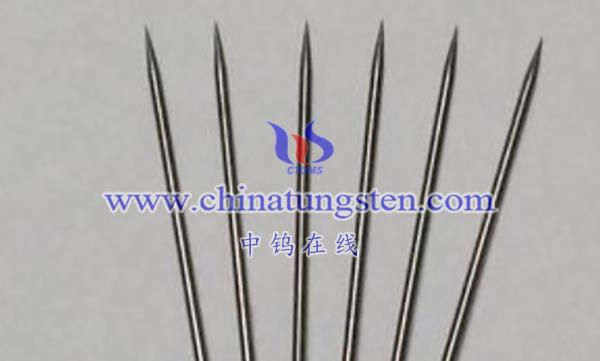
The ground tungsten pin for wafer testing is a probe used for wafer testing, and its tip has been specially ground. This design aims to increase the sharpness of the probe and reduce the radius of the tip to enable more delicate and high-precision testing. By sharpening, the tip of the probe can be made sharper, making it suitable for applications requiring high-precision testing, especially in the field of microelectronics.
Some features and application areas include:
1. Improved sharpness: Sharpening can make the tip of the probe sharper, thereby achieving smaller area electrical connections and higher-precision testing.
2. High-precision testing: Ground tungsten pins are often used in applications that require high-precision testing, such as testing of tiny circuits in the field of microelectronics.
3. Microelectronics applications: In the field of microelectronics, probes need to be sharp enough to ensure accurate electrical connections on tiny circuit components.
4. Reduce wear: Sharpening helps reduce wear on the probe tip and prolongs the service life of the probe.
5. High-density testing: Due to the sharp design, the ground tungsten pin is suitable for high-density test layouts.
More details of tungsten needles, please visit website: http://tungsten.com.cn/tungsten-needles-and-pins.html
Please contact CHINATUNGSTEN for inquiry and order of tungsten needles:
Email: sales@chinatungsten.com
Tel.: +86 592 5129595