The application of high-density alloys in microelectronic packaging mainly includes the following aspects:
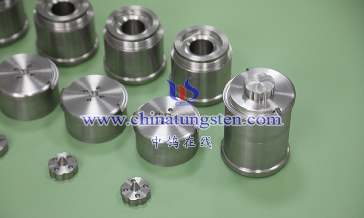
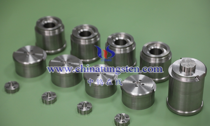
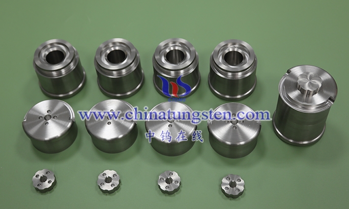
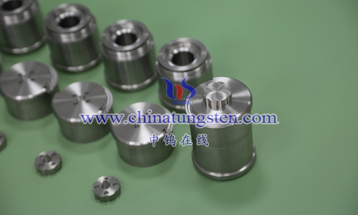
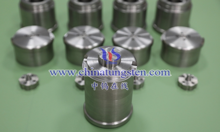
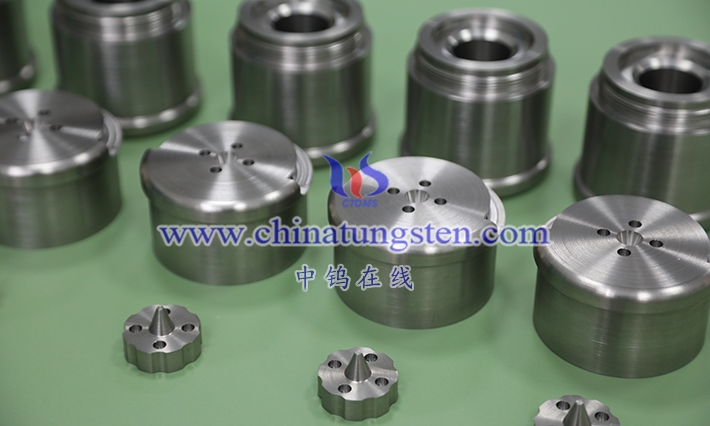
- Chip carrier and support: High-density alloys can be used to make chip carriers and support structures to carry and fix the chip to ensure the stability and reliability of the chip during the packaging process.
- Heat sinks and radiators: High-density alloys have excellent thermal conductivity and can be used to make heat sinks and radiators for microelectronic packaging. These components can effectively conduct the heat generated by the chip away, ensuring the stability and reliability of the chip during operation.
- Pins and connectors: High-density alloys can be used to make pins and connectors for microelectronic packages, which are used for electrical connections and signal transmission between chips and other components.
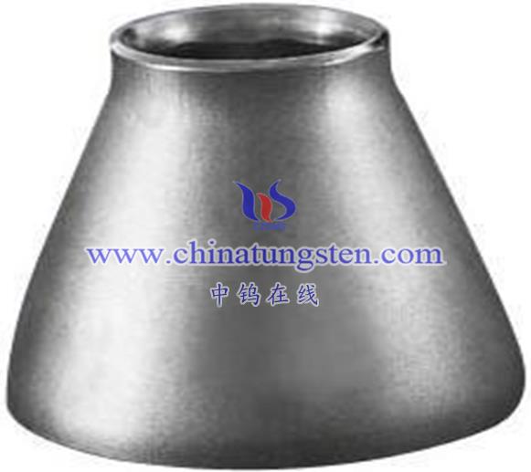
- Structural parts and shells: High-density alloys can be used to make structural parts and shells of microelectronic packages to protect chips and other components and ensure the stability and reliability of the entire package.
- Electromagnetic shielding: High-density alloy has excellent electromagnetic shielding properties and can be used to make electromagnetic shielding covers for microelectronic packaging to protect chips from electromagnetic interference and radiation.
In short, high-density alloys have a wide range of applications in microelectronic packaging and can be used in many aspects such as carrying chips, conducting heat, transmitting signals, and protecting chips and other components. These applications can improve the performance and reliability of microelectronic packaging and promote the development of microelectronics technology.
More details of tungsten alloy product, please visit website: http://tungsten-alloy.com/
Please contact CHINATUNGSTEN for inquiry and order of tungsten carbide:
Email: sales@chinatungsten.com
Tel.: 86 592 5129595