The specifications of tungsten probes for LED wafer test may vary by manufacturer and specific application. These specifications typically include the size, shape, electrical properties, etc. of the probe. Here are some general specifications:
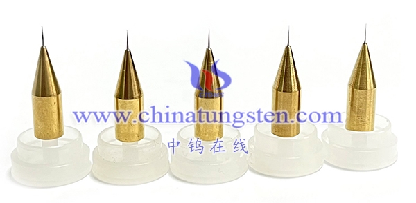
1. Size: Including the length, diameter and other dimensional parameters of the probe. Wafer test probes often need to be very small in size to fit the tiny circuit components on tiny wafers.
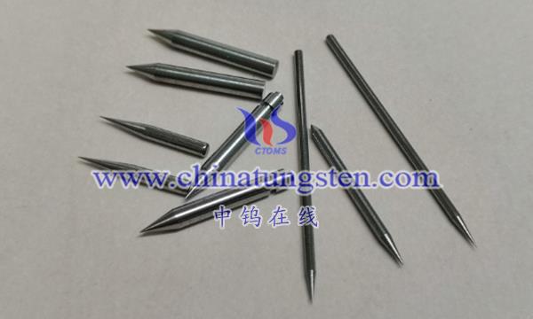
2. Shape: The shape of the probe can vary depending on the application. Common shapes include cones, spheres, sharp tips, etc. The choice of shape may depend on the specific requirements of the test and the circuit design on the wafer.
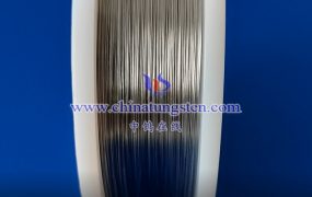
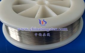
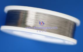
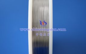
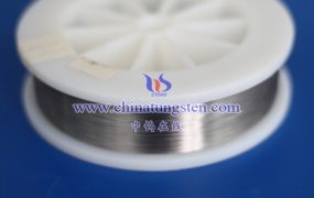
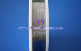
3. Material: Usually tungsten or tungsten alloy, in which alloying elements doped may provide specific properties, such as increased hardness, electrical conductivity, etc.
4. Electrical properties: including performance parameters such as resistance, conductivity, current capacity, etc. These parameters affect the performance of the probe during electrical connection and testing.
5. Wear characteristics: Involves the wear rate and life of the probe. This is a critical specification, especially considering that LED wafer test is a highly repetitive process.
6. Temperature range: The temperature stability of the probe and its ability to maintain performance under different temperature conditions. This may be a critical specification in some special applications.
7. Automation adaptability: For the design of automated testing systems, ensure that probes can adapt to the automated testing process.
More details of tungsten probes, please visit website: http://tungsten.com.cn/tungsten-needles-and-pins.html
Please contact CHINATUNGSTEN for inquiry and order of tungsten needles:
Email: sales@chinatungsten.com
Tel.: +86 592 5129595