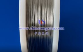
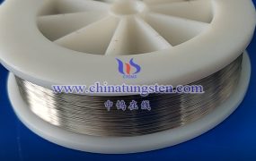
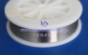
There are many types of tungsten probes for LED wafer test, and the choice often depends on the specific test needs and application. The following are some common types:
1. Tapered Probe: This type of probe has a tapered tip and is suitable for testing applications that require small area contact. Tapered probes are typically used on high-density wafers.
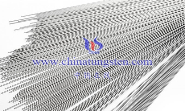
2. Spherical probe: The tip of the probe is spherical, providing a relatively large contact area. Spherical probes are suitable for some test applications where contact area requirements are not so critical.
3. Sharp Probe: This type of probe has a very sharp tip and is often used for high-precision testing that requires very small contact points, such as in the field of microelectronics.
4. Graduated Probes: These probes have tiny graduations or markings on the tip that are used to measure or locate specific test points.
5. Sharpened probe: It has a specially processed sharpened tip to improve the sharpness of the probe and reduce wear.
6. Automatic test probe: The probe designed for the automatic test system has the characteristics of adapting to the automated test process.
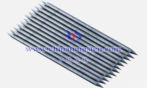
7. High temperature test probe: Probe specially designed for testing in high temperature environment.
8. Multi-channel probe: Equipped with multiple probe channels, it can test multiple test points or multiple wafers at the same time.
9. Specially shaped probes: Specially shaped probes designed according to specific testing requirements.
More details of tungsten probes, please visit website: http://tungsten.com.cn/tungsten-needles-and-pins.html
Please contact CHINATUNGSTEN for inquiry and order of tungsten needles:
Email: sales@chinatungsten.com
Tel.: +86 592 5129595
