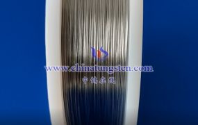
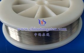
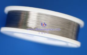
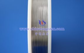
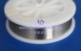
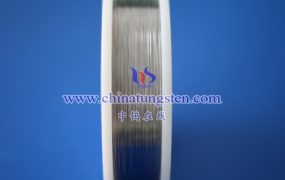
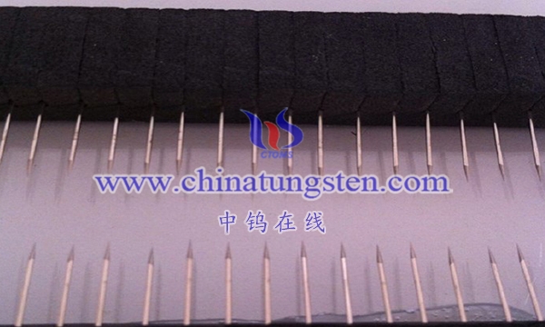
The tapered tungsten probe tip is a probe used for wafer testing with a tapered tip. This type of probe is typically used on high-density wafers where the distance between test points is very small and a small area of contact is required. The tapered tip design facilitates precise and efficient electrical connections to tiny test points.
Some features and application areas include:
1. Small area contact: The tip design of the tapered probe enables it to make electrical connection with the test point in a very small area. This is important for tiny circuit components on high-density wafers.
2. High-precision testing: Conical probes are often used in applications that require high-precision testing, such as in the field of microelectronics. Its sharp tip helps make accurate electrical connections.
3. Suitable for small-size wafers: The tapered tungsten probe tip is suitable for small-size wafers where the distance between test points is very close.
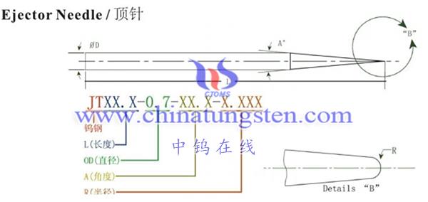
4. High-density testing: Due to the design of the tapered probe, it can accommodate high-density test layouts while maintaining a small contact area.
5. Microelectronics applications: Tapered tungsten probe tips are often used in the field of microelectronics to test tiny circuits on integrated circuit chips.
More details of tungsten probes, please visit website: http://tungsten.com.cn/tungsten-needles-and-pins.html
Please contact CHINATUNGSTEN for inquiry and order of tungsten needles:
Email: sales@chinatungsten.com
Tel.: +86 592 5129595