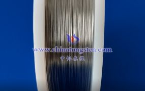
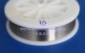
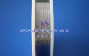
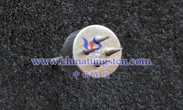
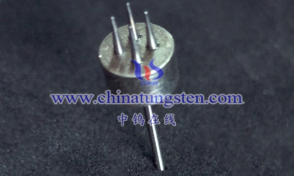
The sharp tungsten probe tip is a probe used for wafer testing, and its tip is designed to be very sharp. This sharp design allows the probe to make high-precision electrical connections to test points in a very small area. Sharp tungsten probe tips are commonly used in test applications that require very high precision, such as in the field of microelectronics.
Some features and application areas include:
1. Very small contact area: The tip of the sharp tungsten probe tip is very sharp and can make electrical connection with the test point in a very small area. This is important for tiny circuit components on high-density wafers.
2. High-precision testing: The sharp design makes the probe very suitable for applications that require high-precision testing, such as testing of tiny circuits in the field of microelectronics.
3. Microelectronics applications: Sharp tungsten probe tips are often used in the field of microelectronics to test tiny circuits on integrated circuit chips.
4. Reduce interference: Since the tip of the probe is very small, it can reduce electrical connection interference with surrounding test points, providing more accurate test results.
5. High-density testing: Due to the sharp design, the probe is able to adapt to high-density test layouts while maintaining a very small contact area.
More details of tungsten probes, please visit website: http://tungsten.com.cn/tungsten-needles-and-pins.html
Please contact CHINATUNGSTEN for inquiry and order of tungsten needles:
Email: sales@chinatungsten.com
Tel.: +86 592 5129595