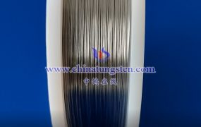
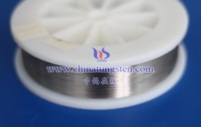
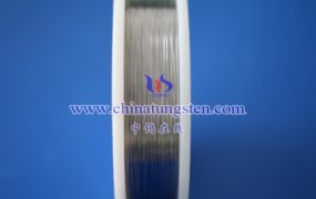
Wafer testing tungsten probe is one of the key testing tools in the fields of semiconductor manufacturing and microelectronics. Its design and performance directly affect the quality and performance of integrated circuits. The characteristics and advantages of tungsten probes for wafer testing will be analyzed in detail below.
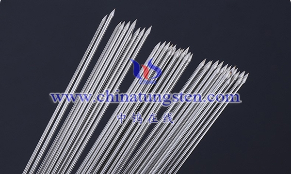
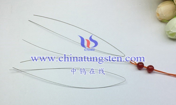
1. Sharpness and precision
The sharpness and precision of wafer test tungsten probes are one of their most important features. The sharpness determines whether the probe can accurately establish electrical connection with the test point, while the accuracy is directly related to the reliability of the test results. Highly sharp probes can establish high-precision electrical connections at tiny test points and are suitable for testing high-density integrated circuits in microelectronics.
2. High temperature stability
Some applications require testing in high-temperature environments, such as testing the electrical performance of chips on a semiconductor production line. Wafer testing tungsten probes usually have good high-temperature stability and can maintain performance under high-temperature conditions to ensure the accuracy of test results.
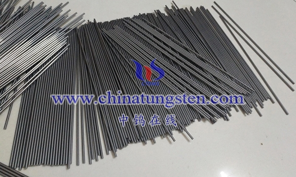
3. Wear resistance and long life
Wafer test tungsten probes need to have good wear resistance because they may frequently come into contact with test points during the test process. Long-life probes can reduce the frequency of replacement and maintenance, improve test efficiency and reduce costs.
4. High-density testing
With the continuous development of integrated circuit technology, the size of circuit components continues to shrink, and the distance between test points is also shrinking, requiring test tungsten probes to adapt to high-density test layouts. This requires a more sophisticated design of the tip of the probe, which can be flexibly operated in a limited space.
5. Automation adaptability
As the degree of automation in semiconductor manufacturing and testing increases, wafer testing tungsten probes need to be adaptable to automation. They can work together with robots or automatic transposition equipment in automatic test systems to achieve an efficient and accurate test process.
6. Multi-channel design
Some applications require testing multiple circuit components or multiple chips simultaneously, which requires multi-channel wafer test tungsten probes. This design can improve testing efficiency, reduce overall testing time, and is suitable for testing needs on large-scale production lines.
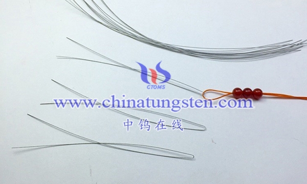
7. Special shapes and customized designs
Some test applications require specially shaped test probes to accommodate specially shaped test points or special application requirements. Some manufacturers offer customized design services and are able to design and manufacture products based on a customer’s specific needs.
8. Diversity of application areas
Wafer testing tungsten probes are widely used in microelectronics, semiconductor manufacturing, integrated circuit testing and other fields. In microelectronics, they are used to test tiny-sized circuit components; in semiconductor manufacturing, they are used to test the electrical performance of chips; in integrated circuit testing, they are used for high-density, high-precision testing requirements.
9. Various tungsten probe types
According to different application requirements, there are many types of tungsten probes for wafer testing, including sharpened designs, special shape designs, multi-channel designs, etc. This diversity allows users to select the appropriate probe type based on specific test requirements.
10. Reliable manufacturer support
Choosing a reliable manufacturer is critical to obtaining high-quality tungsten probes for wafer testing. Some manufacturers provide complete technical support, after-sales service and customized designs to ensure that customers receive the best performance and service during use.
11. Compliance and Quality Certification
Wafer testing tungsten probes need to comply with a series of industry standards and quality certifications during production and use. Compliance and quality certification ensure reliability and stability during the production and use of probes.
12. Environmental protection and sustainability
Some manufacturers focus on environmental protection and sustainability, striving to reduce resource consumption and environmental impact in the production process. These environmental awareness are very important for corporate social responsibility and sustainable development.
More details of tungsten probes, please visit website: http://tungsten.com.cn/tungsten-needles-and-pins.html
Please contact CHINATUNGSTEN for inquiry and order of tungsten needles:
Email: sales@chinatungsten.com
Tel.: +86 592 5129595