However, the tungsten-rhenium contact probe also has the following disadvantages:
1. High cost: Since the manufacturing process of the tungsten-rhenium contact probe is relatively complicated and requires the use of high-precision grinding and polishing equipment, its cost is relatively high.
2. Regular maintenance is required: In order to ensure the safety and stability of the tungsten-rhenium contact probe, regular maintenance and maintenance are required, which increases the cost of use.
3. High requirements for operation: Since the tungsten-rhenium contact probe has a high precision, the operation requirements are also high, and professionally trained personnel are required to perform correct operation and maintenance.
4. Application fields of tungsten-rhenium contact probes
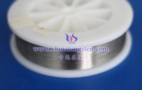
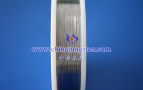
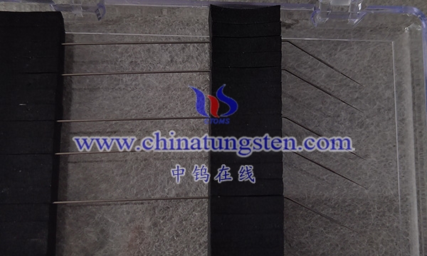
Tungsten-rhenium contact probes are widely used in semiconductor testing, wafer testing, PCB testing and other fields. In semiconductor testing, tungsten-rhenium contact probes are used to test the performance and reliability of chips; in wafer testing, tungsten-rhenium contact probes are used to detect the surface quality and defects of wafers; in PCB testing, tungsten-rhenium contact probes are used to detect the line integrity and electrical performance of PCB boards. In addition, tungsten-rhenium contact probes can also be used in battery testing, thin film testing and other fields.
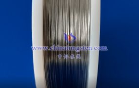
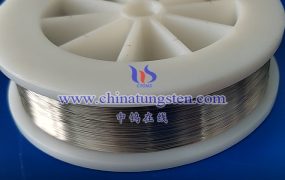
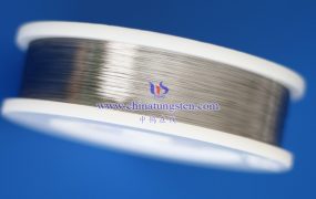
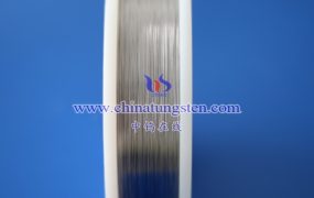
More details of tungsten probes, please visit website: http://tungsten.com.cn/tungsten-needles-and-pins.html
Please contact CHINATUNGSTEN for inquiry and order of tungsten needles:
Email: sales@chinatungsten.com
Tel.: +86 592 5129595