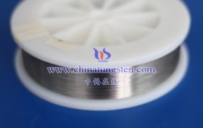
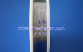
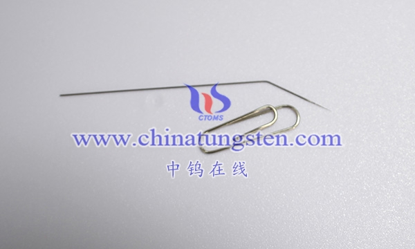
The application of tungsten needles in electron beam manufacturing is mainly reflected in electron beam evaporation coating machines (EBEP for short), which is a coating technology widely used in materials science, optics, semiconductors and electronic manufacturing.
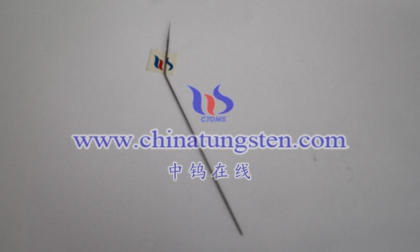
In EBEP, tungsten needles are used as electron sources, and their working principle can be summarized as the following steps:
- Emission of electrons: When the tungsten needle is heated to a high temperature, it emits electrons. These electrons have enough energy to propagate and remain stable in a vacuum.
- Electric field acceleration: By setting an accelerating electric field, the electrons emitted by the tungsten needle are accelerated to a higher speed. This gives the electrons enough energy to bombard the target material.
- Target bombardment: When high-speed electrons bombard the target material, the molecules or atoms on the surface of the target material will gain enough energy to evaporate and detach from the target material. This process will produce a large number of gas molecules or atoms, which are then deposited on the surface of the substrate to form a thin film.
EBEP coating technology has many advantages, such as being able to be carried out in a high vacuum environment, being able to accurately control the thickness and composition of the film, and being able to achieve large-area uniform coating. Therefore, this coating technology is often used to manufacture optical devices, solar cells, decorations or for material surface modification.
In specific applications, the quality and performance of the tungsten needle have an important influence on the effect of EBEP. For example, the emission current, electron energy distribution and stability of the tungsten needle will affect the quality and efficiency of the coating. Therefore, it is very important for researchers and engineers engaged in EBEP coating technology to select the right tungsten needle and optimize its performance.
In general, the application of tungsten needles in the field of electron beam manufacturing demonstrates its important position in the high-tech industry, especially in promoting the development of materials science, optics, semiconductors and electronic manufacturing.
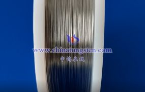
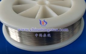
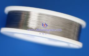
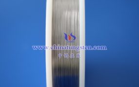
More details of tungsten probes, please visit website: http://tungsten.com.cn/tungsten-needles-and-pins.html
Please contact CHINATUNGSTEN for inquiry and order of tungsten needles:
Email: sales@chinatungsten.com
Tel.: +86 592 5129595