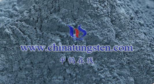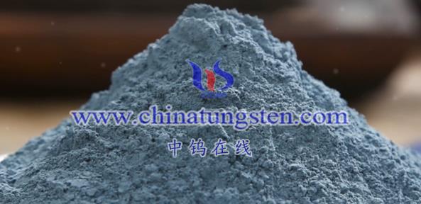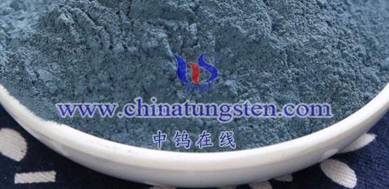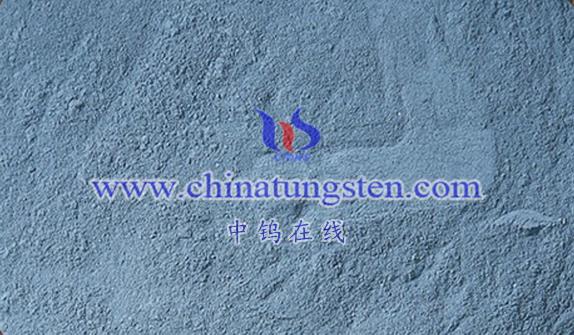
Nano tungsten oxide (WO₃) semiconductor sensing refers to a technology that uses nanoscale tungsten oxide as a sensitive element to detect and measure specific gases by monitoring changes in its electrical resistance or other electrical properties. This sensing technique leverages the unique properties of nanomaterials and the gas-sensitive effect of semiconductors, offering advantages such as high sensitivity, fast response, and good selectivity. Below is a detailed explanation:
- Characteristics of Nano Tungsten Oxide
- High Specific Surface Area
Nano tungsten oxide has an extremely high surface area, enabling it to adsorb more gas molecules, thus enhancing the sensor’s sensitivity. - Abundant Surface Defects
Its surface contains numerous defects and vacancies, which serve as active sites for gas adsorption and reaction, further improving sensor performance. - n-Type Semiconductor Properties
Nano tungsten oxide is an n-type semiconductor whose electrical conductivity changes with the type and concentration of gases adsorbed on its surface, making it an ideal material for gas sensors.
- Working Principle of Nano Tungsten Oxide Semiconductor Sensing
The working principle is primarily based on the semiconductor gas-sensitive effect. When gas molecules are adsorbed onto the surface of nano tungsten oxide, they exchange electrons with the material, causing changes in its electrical conductivity.
- Oxidizing Gases (e.g., O₂, NO₂): These gases capture electrons from the material’s surface, forming negatively charged ions. This reduces the number of free electrons, increasing the material’s resistance.
- Reducing Gases (e.g., H₂, CO): These gases donate electrons to the material, forming positively charged ions. This increases the number of free electrons, decreasing the material’s resistance.
By measuring the changes in electrical resistance or other properties, the sensor can detect the type and concentration of the gas.
- Applications of Nano Tungsten Oxide Semiconductor Sensing
- Environmental Monitoring
Detects atmospheric pollutants such as nitrogen oxides (NOx) and sulfur oxides (SOx). - Industrial Safety
Monitors toxic and hazardous gas leaks, such as ammonia (NH₃) and hydrogen sulfide (H₂S), ensuring industrial safety. - Medical and Healthcare
Used in breath analysis to monitor specific gases for disease diagnosis. - Energy Sector
Can also serve as an anode material in lithium-ion batteries, offering high energy density and stable cycling performance.
- Advantages of Nano Tungsten Oxide Semiconductor Sensing
- High Sensitivity
Capable of detecting gases at very low concentrations. - Fast Response
Quickly responds to changes in gas concentrations. - Good Selectivity
Optimizing the material’s structure and composition allows selective detection of specific gases. - Excellent Stability
Maintains stable performance even at high temperatures.
- Limitations of Nano Tungsten Oxide Semiconductor Sensing
- Humidity Sensitivity
The performance can be affected by environmental humidity. - Need for Improved Selectivity and Stability
Further improvements are necessary to meet stringent application requirements. - High Production Costs
The fabrication of nanomaterials is complex, leading to higher production costs.
Summary
Nano tungsten oxide semiconductor sensing is a promising gas-sensing technology with broad applications in environmental monitoring, industrial safety, medical diagnostics, and energy. As advancements in nanotechnology and semiconductor technology continue, this sensing method is expected to achieve further improvements in performance and cost-effectiveness, providing reliable solutions for a wide range of gas detection needs.
More details of tungsten oxide product, please visit website: tungsten-oxide.com
Please contact CHINATUNGSTEN for inquiry and order of tungsten oxide:
Email: sales@chinatungsten.com
Tel.: 86 592 5129595
