Semiconductor crucibles are key consumables used to pull single crystal silicon rods in semiconductor manufacturing. They are usually made of high-purity quartz sand and have the characteristics of high temperature resistance, high purity, and low bubble rate. They are one of the core tools in semiconductor silicon wafer production.
- Definition and Structure
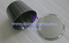
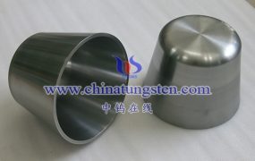
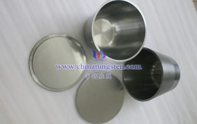
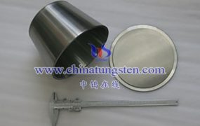
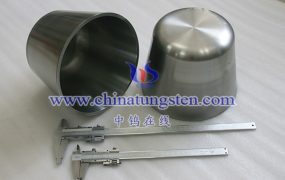
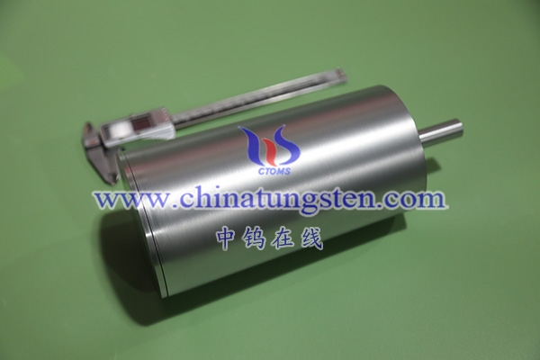
Definition: Semiconductor crucible is a high-purity quartz crucible specially designed for the semiconductor industry. It is used to hold molten silicon liquid and pull single crystal silicon rods through the Czochralski method.
Structure: It is usually divided into an outer layer (opaque layer) and an inner layer (transparent layer). The outer layer is a high-density area containing a large number of bubbles to enhance thermal insulation; the inner layer is a 3-5mm transparent layer with low bubble density to ensure the purity of the area in contact with the silicone liquid.
- Performance requirements
High purity:
of SiO₂ must be greater than 99.998%, the impurity content must be less than 10ppm, and the gas-liquid inclusion content must be less than 100ppm.
The inner layer of high-purity semiconductor synthetic quartz crucible requires a purity of 8N or above.
High temperature resistance:
It can be used for a long time below 1450°C, meeting the temperature requirements of the single crystal silicon pulling process.
Low bubble rate:
The inner bubble density is low, which prevents the release of bubbles and causes defects in the single crystal silicon rod.
Thermal stability:
Good thermal shock stability ensures no cracking during high temperature and cooling.
- Application fields
Semiconductor silicon wafer production: used to draw high-purity single-crystal silicon rods, which are the core materials for manufacturing integrated circuits and microelectronic devices.
Photovoltaic industry: Some quartz crucibles for photovoltaics also use similar technology, but the purity requirements are relatively low.
- Manufacturing process
Raw material selection:
The inner layer is made of synthetic quartz sand and the outer layer is made of natural quartz sand, ensuring the high purity of the inner layer and the thermal insulation of the outer layer.
Molding process:
High-purity quartz sand is melted at high temperature by arc method to form crucible blanks, which are then mechanically processed and chemically treated to remove impurities and bubbles.
Quality Control:
Strictly control factors such as the number of bubbles, impurity content, hydroxyl content, etc. to ensure the quality and performance of the crucible.
- Technical Challenges and Development Trends
Technical Challenges:
The preparation technology of large-size crucibles is still an industry secret, and the core parameters need to be perfectly balanced.
There is a gap between domestic companies and some developed countries in terms of product stability and microbubble control.
Development Trends:
Large size: As the size of semiconductor silicon wafers increases, the demand for large-sized high-purity quartz crucibles increases.
Domestic substitution: As the global semiconductor industry shifts to China, the market share of domestic semiconductor quartz crucibles is expected to increase.
Technological innovation: Research and develop quartz crucibles with higher purity and lower bubble rate to meet the needs of advanced processes.
- Market and Industry
Market demand: With the development of the semiconductor industry, the market demand for quartz crucibles for semiconductors continues to grow.
Industrial chain: The upstream is the high-purity quartz sand supplier, and the downstream is the semiconductor silicon wafer manufacturer.
Industry barriers: high technical threshold, high industry concentration, and leading companies master core preparation technologies.
======================================================================
Customized R&D and Production of Tungsten, Molybdenum Products
Chinatungsten Online and CTIA GROUP LTD have been working in the tungsten industry for nearly 30 years, specializing in flexible customization of tungsten and molybdenum products worldwide, which are tungsten and molybdenum design, R&D, production, and overall solution integrators with high visibility and credibility worldwide.
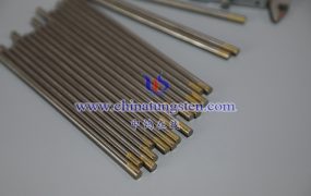
Chinatungsten Online and CTIA GROUP LTD provide products mainly including: tungsten oxide products, such as tungstates such as APT/WO3; tungsten powder and tungsten carbide powder; tungsten metal products such as tungsten wire, tungsten ball, tungsten bar, tungsten electrode, etc.; high-density alloy products, such as dart rods, fishing sinkers, automotive tungsten crankshaft counterweights, mobile phones, clocks and watches, tungsten alloy shielding materials for radioactive medical equipment, etc.; tungsten silver and tungsten copper products for electronic appliances. Cemented carbide products include cutting tools such as cutting, grinding, milling, drilling, planing, wear-resistant parts, nozzles, spheres, anti-skid spikes, molds, structural parts, seals, bearings, high-pressure and high-temperature resistant cavities, top hammers, and other standard and customized high-hardness, high-strength, strong acid and alkali resistant high-performance products. Molybdenum products include molybdenum oxide, molybdenum powder, molybdenum and alloy sintering materials, molybdenum crucibles, molybdenum boats, TZM, TZC, molybdenum wires, molybdenum heating belts, molybdenum spouts, molybdenum copper, molybdenum tungsten alloys, molybdenum sputtering targets, sapphire single crystal furnace components, etc.
If you are interested in related products, please contact us:
Email: sales@chinatungsten.com
Tel: +86 592 5129696 / 86 592 5129595