Chapter 18 Coated Cemented Carbide
18.1 Introduction: The concept and importance of coated cemented carbide
In the field of modern industrial manufacturing, cemented carbide, as a high-performance material, has become a core component of cutting tools, wear-resistant parts and precision molds. However, with the increasing complexity of processing conditions, such as high temperature, high-speed cutting, dry processing and higher requirements for material durability, relying solely on the performance of the cemented carbide substrate is often difficult to meet multi-dimensional needs. This has led to the rapid development of coated cemented carbide technology. By depositing one or more layers of functional films on the surface of the cemented carbide substrate, the coated cemented carbide not only retains the toughness and strength of the substrate, but also significantly improves the surface wear resistance, heat resistance and chemical stability, enabling it to exhibit excellent performance in extreme environments. This chapter will systematically explore the physical and chemical properties of coated cemented carbide, coating process technology and its applications in cutting, wear resistance and other fields, aiming to provide practitioners and researchers with a comprehensive and in-depth reference.
The rise of coated cemented carbide stems from the materials science revolution of the mid-20th century. As early as the late 19th century, the invention of cemented carbide ( a tungsten-cobalt alloy by German scientist Karl Schroter in 1909) marked a major breakthrough in materials engineering. However, at the time, cemented carbide primarily relied on the properties of the substrate and was prone to failure in high temperatures or corrosive environments. In 1953, the Swiss company Balzers pioneered the use of chemical vapor deposition (CVD) technology to deposit a TiC coating on cemented carbide tools . This coating, approximately 5 μm thick and with a hardness of HV 3000, significantly improved wear resistance and extended tool life by 3-5 times. This innovation pioneered coating technology and was quickly adopted by the tool manufacturing industries in Germany and the United States.
The emergence of physical vapor deposition (PVD) technology in the 1960s further advanced coating development. In 1962, American scientist Donald M. Mattox invented ion plating. In 1970, German tool manufacturer Kennametal developed a TiN coating with a thickness of 2-4 μm , reducing the coefficient of friction to below 0.4, suitable for medium cutting speeds. During this period, coating technology moved from the laboratory to commercialization, with its share of the global tool market increasing from 5% to 20%. In the 1970s, multilayer coatings (such as TiC / TiN /Al2O3) were developed, combining the advantages of each layer. Coatings can reach thicknesses of up to 10 μm and heat resistance exceeding 1000°C. In the 21st century, nanocomposite coatings (such as nc-AlTiN /a-Si3N4) matured. In 2005, Swedish company Sandvik launched a nanocoated tool with a hardness of HV 4000 and a thickness of 1-5 μm , suitable for high-speed dry cutting. China’s research on coated cemented carbide began in the 1980s. Standards such as the GB/T 18376 series standardized coating performance testing, driving the transformation of domestic industries from import dependence to independent innovation. Currently, the global market for coated cemented carbide exceeds US$50 billion, with an annual growth rate of approximately 5%. The aerospace and automotive manufacturing sectors account for over 70% of this market. The introduction of coating technology not only extends the life of cemented carbide tools (by an average of 2-5 times), but also reduces data generation and processing energy consumption, improving efficiency and environmental friendliness. For example, in the machining of automotive engine parts, coated cemented carbide tools can reduce cutting energy consumption by 20%-30%. In agricultural machinery, coated cemented carbide wear-resistant parts (such as plowshares) can extend the soil wear life from 500 hours to over 1,000 hours, significantly improving tillage efficiency.
The importance of coated cemented carbide is also reflected in its strategic value. In the global supply chain, as a major cemented carbide producer (accounting for more than 50% of the world’s output), coating technology has become the key to improving product competitiveness. According to data from the China Nonferrous Metals Industry Association, since 2015, the export volume of coated cemented carbide has increased by an average of 8% per year, mainly due to the localization of PVD and CVD processes. The coating not only solves the limitations of the cemented carbide substrate (such as oxidation sensitivity and high friction coefficient), but also optimizes the interface bonding strength. The interface energy is usually controlled at 2-5 J/m² to avoid delamination. This development history reflects the transformation of materials science from a single matrix to a composite structure, laying the foundation for future intelligent coatings (such as self-healing coatings). This chapter starts with the definition of coating and gradually unfolds a comprehensive exploration of its performance, process and application, aiming to reveal how coating technology reshapes the application landscape of cemented carbide.
18.1.1 Definition and Development History of Coated Cemented Carbide
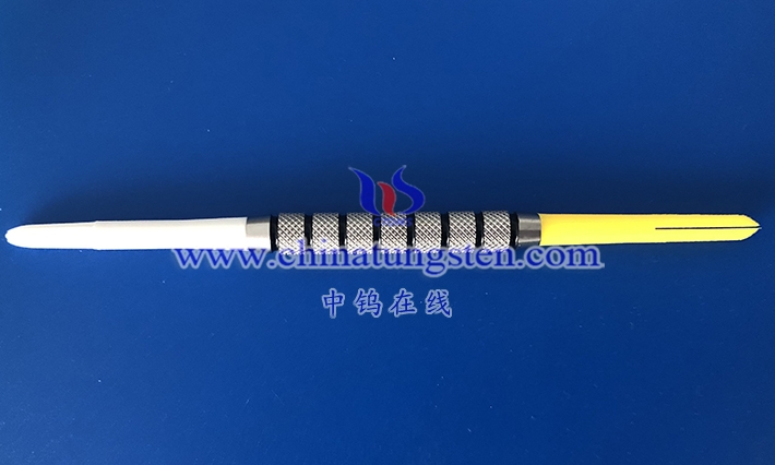
Coated cemented carbide refers to a composite structure in which a thin film of material is deposited onto the surface of a cemented carbide substrate (such as tungsten-cobalt alloy or tungsten-titanium-cobalt alloy) via methods such as physical vapor deposition (PVD) or chemical vapor deposition (CVD). This film is typically 1-15 microns thick. The substrate provides mechanical support and toughness, while the coating enhances surface hardness, wear resistance, and heat resistance. The cemented carbide substrate consists of tungsten carbide (WC) particles (1-20 μm in diameter ) as the hard phase and cobalt (Co) or nickel (Ni) as the binder phase (5-15%). Produced through a powder metallurgy process, it exhibits high flexural strength (1800-2500 MPa) and hardness (HRA 85-92). Coating materials primarily include nitrides ( TiN , CrN ), carbides ( TiC ), and oxides (Al2O3). By optimizing their composition and structure, they achieve customized enhancements to the substrate’s properties. For example, TiAlN coating can increase the heat resistance temperature of the substrate from 600°C to over 1000°C, making cemented carbide perform better in high-speed cutting.
The development of coated cemented carbide can be traced back to the materials science revolution of the mid-20th century. In 1909, German scientist Karl Schroter invented tungsten-cobalt cemented carbide, marking a breakthrough in powder metallurgy. However, early cemented carbide suffered from oxidation and adhesive wear during high-temperature cutting. In 1953, Swiss company Balzers pioneered the use of chemical vapor deposition (CVD) technology to deposit a titanium carbide ( TiC ) coating on cemented carbide tools . This coating, approximately 5 μm thick and with a hardness of HV 3000, significantly improved wear resistance and extended tool life by 3-5 times. This innovation pioneered coating technology and was quickly adopted by the tool manufacturing industries in Germany and the United States, marking the shift from bare substrates to coated composites.
The emergence of physical vapor deposition (PVD) technology in the 1960s further advanced coating development. In 1962, American scientist Donald M. Mattox invented ion plating technology. In 1970, German tool manufacturer Kennametal developed a titanium nitride ( TiN ) coating with a thickness of 2-4 μm , reducing the friction coefficient to below 0.4, suitable for medium cutting speeds. During this period, coating technology moved from the laboratory to commercialization, and its share of the global tool market increased from 5% to 20%. In the 1970s, multilayer coatings (such as TiC / TiN /Al2O3) were developed, combining the advantages of each layer. Coating thicknesses reached 10 μm , with heat resistance exceeding 1000°C. In the 1980s, low-temperature PVD technologies (such as arc ion plating) matured, reducing deposition temperatures to 400-500°C, avoiding thermal deformation of the cemented carbide substrate. China’s research into coated cemented carbide began in the 1980s. In the early 1990s, Zhuzhou Cemented Carbide Factory introduced CVD technology to produce TiC- coated cutting tools, which spurred localization. In the 21st century, nanocomposite coatings (such as nc-AlTiN /a-Si3N4) matured. In 2005, Swedish company Sandvik launched nanocoated cutting tools with a hardness of HV 4000 and a thickness of 1-5 μm , suitable for high-speed dry cutting. Chinese companies such as Xiamen Jinlu and Zhuzhou Diamond have achieved localization, with exports of coated cemented carbide growing at an average annual rate of 10%.
The evolution of coating technology has not only overcome the limitations of cemented carbide but also expanded its application, from cutting tools to wear-resistant parts, creating an $80 billion global market. This development reflects the shift in materials science from single substrates to composite structures, laying the foundation for future intelligent coatings, such as self-healing coatings.
18.1.2 Mechanism of Coating Action in Cemented Carbide
The mechanisms of action of coatings on cemented carbide are primarily based on three aspects: physical barrier, chemical protection, and mechanical reinforcement. First, from a physical perspective, coatings reduce wear by increasing surface hardness (HV 2000-4000) and reducing the coefficient of friction (0.1-0.4). The hardness of the cemented carbide substrate (such as YG8) is HRA 83-85, and the coefficient of friction reaches 0.5 during high-speed cutting, leading to heat accumulation and adhesive wear. Coatings such as TiAlN form a dense protective layer, increasing the hardness to HV 3200 and reducing the coefficient of friction to 0.2, thereby reducing heat generation by 20-30%. This mechanism is explained by a thermal diffusion model: the coating’s low thermal conductivity (5-10 W/ m·K ) blocks heat flow, lowering the substrate temperature by 100-200°C and preventing softening of the cobalt phase. Furthermore, the coating improves fatigue resistance, reducing the crack growth rate by 50% under cyclic loading and extending tool life by 2-5 times.
Secondly, from a chemical perspective, the coating provides an anti-oxidation and anti-corrosion barrier. Cemented carbide substrates are susceptible to oxidation at high temperatures (>800°C), with dissolution of the cobalt phase leading to the shedding of WC particles. However, coatings such as Al2O3 exhibit high chemical stability, remaining intact above 1000°C and inhibiting the oxidation reaction rate by over 90%. TiN coatings, through their chemical inertness, reduce reactions with the workpiece material, thereby reducing chemical wear. In corrosive environments, such as agricultural wear parts in saline soils, CrN coatings provide electrochemical protection, reducing corrosion current density to 10^{-7} A/cm² and extending coating life by 2-3 times. The chemical mechanism can be described by the Arrhenius equation: an increase in the activation energy of the coating by 20-50 kJ/mol leads to an exponential decrease in the oxidation rate. Furthermore, the coating optimizes interfacial chemical compatibility by reducing substrate-coating diffusion reactions through an intermediate layer (such as TiC ), with the interface thickness controlled to 0.1-0.5 μm .
Finally, from a mechanical perspective, the coating enhances the substrate’s toughness and impact resistance. The brittleness of cemented carbide (flexural strength of 1800-2500 MPa) is mitigated by the coating’s buffering properties. Multilayer coatings (such as TiN / TiCN /Al2O3) utilize interlayer interfaces to disperse stress, reducing crack growth rates by up to 50%. For example, in impact tests, the crack length of the bare substrate was 0.2 mm, while that of the coated version was only 0.1 mm. The mechanical mechanism is based on stress field theory, with the coating’s modulus (E 200-400 GPa ) matching that of the substrate, reducing interfacial stress concentration. Furthermore, the coating improves thermal stress distribution, bringing the coefficient of thermal expansion (CTE) closer to that of the substrate (CTE 4-6×10^{-6}/K), reducing the risk of thermal cracking.
These mechanisms work synergistically. In practical applications, such as machining aviation titanium alloys, coated carbide tools can achieve tool life over three times longer than bare substrates, while increasing cutting speeds from 150 m/min to 300 m/min. This not only improves efficiency but also reduces energy consumption and emissions, promoting green manufacturing. In the wear-resistant parts sector, the mechanisms of coated carbide also include a self-lubricating effect, reducing frictional heat generation and extending tool life by 1.5-2 times.
18.1.3 Comparison of Coated Carbide and Bare Carbide
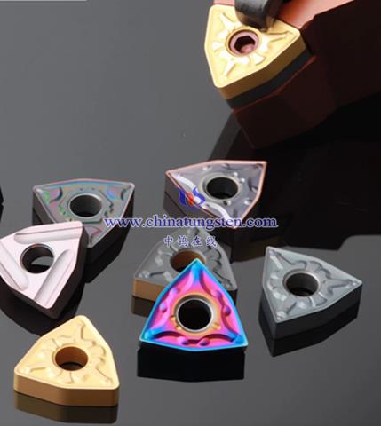
Coated cemented carbide differs significantly from bare carbide in terms of performance, application, economics, environmental friendliness, and future potential. First, from a performance perspective, bare carbide (e.g., YG8) has a hardness of HRA 83-85, a flexural strength of 2000 MPa, and a heat resistance of 700-800°C. However, its surface is susceptible to oxidation and wear, resulting in a short service life in high-speed cutting (100-200 meters for cutting steel). Coated carbide (e.g., YG8 + TiAlN ) has a surface hardness of HV 3000-3500, heat resistance of 1000°C, a friction coefficient reduction of 0.3, and a service life extended by 3-5 times (500-1000 meters for cutting). However, the risk of coating delamination (adhesion <50 MPa) must be controlled through interface optimization (e.g., ion bombardment pretreatment). In addition, the coating also improves fatigue resistance. The crack growth rate of the bare substrate under cyclic impact is 0.5 mm/h, while that of the coated version is reduced to 0.2 mm/h, and the thermal conductivity is reduced by 20%.
Secondly, in terms of application scenarios, the bare substrate is suitable for low-speed, low-temperature machining (such as rough turning cast iron, cutting speed 100 m/min), with low cost (10-20 yuan per piece), but limited wear resistance, making it suitable for general machining. The coated version is suitable for high-speed, dry cutting (such as aviation titanium alloy, cutting speed 300 m/min), with strong durability, but requires precision equipment support, suitable for high-end manufacturing. The bare substrate of cemented carbide agricultural wear-resistant parts has a service life of HB 450 and a service life of 500 hours; after coating, it has a service life of HB 500 and a service life of 800 hours, reducing replacement frequency by 30% and improving farming efficiency. In the mold field, the bare substrate is used for simple stamping (pressure 500 MPa), while the coated version is used for high-precision cold heading (pressure 1000 MPa), and the surface finish is improved by 20%.
In terms of economics, bare substrates have lower production costs (powder metallurgy is simpler), but require more maintenance, resulting in a higher total cost of ownership. Coatings increase PVD/CVD process costs (an additional 5-10 yuan per piece), but offer a longer overall lifespan, reducing total costs by 20-30%. For example, a batch of 1,000 tools would cost 20,000 yuan for bare substrates (with a lifespan of 100 hours), while coated versions would cost 25,000 yuan (with a lifespan of 300 hours), resulting in a 33% reduction in unit cost. Environmentally, coatings reduce cutting fluid usage (by 50%), promoting green manufacturing. Bare substrates, on the other hand, require more coolant, increasing the environmental burden and waste disposal costs (increasing by 10% annually). Regarding corrosion resistance, bare substrates are susceptible to acid and alkali corrosion (corrosion rate of 0.1 mm/year), while coated versions (such as CrN ) reduce this to 0.01 mm/year, making them suitable for humid environments.
Finally, in terms of future potential, coated cemented carbide has more advantages and can be further improved through nanotechnology (such as HV 4000 and above), while bare substrates are difficult to break through due to substrate limitations. Overall, coated cemented carbide has obvious advantages in high-temperature and high-wear scenarios, but interface bonding needs to be optimized to avoid delamination, while bare substrates are suitable for economical applications. The choice depends on the specific working conditions. For example, cutting tools are preferentially coated (efficiency improvement of 50%), while general molds can choose bare substrates (cost savings of 20%). In the future, with the development of AI and intelligent coatings, this comparison will further tilt towards coatings. It is estimated that by 2030, the market share of coated cemented carbide will reach 90%.
As a key innovation in modern materials engineering, coated cemented carbide has become one of the core technologies for improving its performance. In applications such as cutting tools, wear-resistant parts, and precision molds, coatings not only extend the service life of the material but also significantly improve processing efficiency and durability. This chapter focuses on the physical and chemical properties of coated cemented carbide. By systematically analyzing the physical and chemical properties, thickness effects, and performance testing methods of coating materials, it aims to provide researchers and engineers with a comprehensive and professional reference framework. The content is based on material science principles, industry standards (such as ISO 513:2012 and GB/T 18376 series), and the latest research data, combined with technical details and actual cases to reveal how coatings optimize the comprehensive performance of cemented carbide. The following discussion will be carried out in a logical order to ensure that the discussion is detailed and rigorous.
18.1.4 Hard alloy coating process
Cemented carbide coating processes are a key branch of modern surface engineering technology. By depositing functional thin films on the surface, they significantly improve wear resistance, heat resistance, corrosion resistance, and mechanical properties. These processes not only extend the service life of cemented carbide but also expand its application in extreme environments. Cemented carbide substrates typically consist of tungsten carbide (WC) as the hard phase and cobalt (Co) as the binder phase. They exhibit high hardness (HRA 85-92) and flexural strength (1800-2500 MPa), but the bare substrate is susceptible to failure in high-temperature or corrosive environments. Coating processes deposit thin films (1-15 μm thick ) through physical, chemical, or combined methods to form a composite structure and optimize substrate performance. According to international standards (such as ISO 513:2012) and domestic standards (such as GB/T 18376.1-2015), coating processes are categorized into physical vapor deposition (PVD), chemical vapor deposition (CVD), atomic layer deposition (ALD), plasma-enhanced chemical vapor deposition (PECVD), thermal spraying, and laser cladding. The choice of process depends on coating thickness, substrate thermal sensitivity, and application environment. For example, PVD is suitable for thin, precision coatings, while CVD is suitable for thick, high-temperature-resistant coatings.
The development of cemented carbide coating processes stems from the materials science revolution of the mid-20th century. In 1953, the Swiss company Balser first used CVD technology to deposit TiC coatings, ushering in the coating era. The emergence of PVD technologies (such as arc ion plating) in the 1960s reduced coating deposition temperatures to 400-600°C, preventing thermal deformation of the substrate. In the 1970s, multilayer coatings (such as TiC / TiN /Al2O3) emerged, combining the advantages of each layer to achieve coating thicknesses of up to 10 μm and heat resistance of up to 1000°C. In the 1980s, low-temperature PVD and PECVD matured, becoming suitable for DLC coatings. In the 21st century, ALD and nanocomposite coating technologies (such as nc-AlTiN ) emerged, reducing coating thicknesses to the nanometer scale and achieving hardnesses exceeding HV 4000. China’s coating technology began developing in the 1980s. Zhuzhou Cemented Carbide Plant introduced CVD technology in the early 1990s. In the 2000s, companies like Xiamen Jinlu developed domestic PVD equipment. Nanocoating achieved breakthroughs in the 2010s, and by 2025, domestic coatings accounted for 80% of the market. These technological advancements not only addressed the limitations of cemented carbide but also promoted advances in green manufacturing and intelligent processing. The following section discusses each process in detail, including its principles, technical parameters, advantages and disadvantages, and applications.
(1.1) What is physical vapor deposition (PVD)?
Physical vapor deposition (PVD) is an advanced surface treatment technology widely used in materials science and manufacturing to deposit a thin, durable coating on a substrate. Simply put, PVD involves physically converting a solid material into a vapor phase, which is then deposited onto the target surface in a vacuum environment. This method differs from chemical vapor deposition (CVD) by utilizing physical processes (such as evaporation or sputtering) to transfer the material, rather than relying on chemical reactions.
thought of as an “evaporation-deposition” process. In a sealed, high-vacuum chamber (typically pressures below 10⁻³ Pa ), the target material (such as titanium, chromium, or their compounds) is heated to extremely high temperatures or vaporized through ion bombardment , transforming it into atomic or molecular vapor. This vapor then moves through the vacuum and condenses on the substrate surface, forming a uniform thin film coating. The entire process typically occurs at low temperatures (300-600°C), which is particularly advantageous for heat-sensitive substrate materials (such as cemented carbide or high-speed steel) because it does not significantly alter the substrate’s inherent properties.
There are several main variations of PVD technology, including:
Evaporative deposition : The material is evaporated by resistive heating or electron beam bombardment, such as traditional vacuum evaporation.
Magnetron sputtering : uses a magnetic field to confine plasma, bombarding the target material to sputter it out, suitable for substrates with complex shapes.
Arc Ion Plating : Utilizes arc discharge to evaporate material, forming a coating with a high ionization rate and stronger adhesion.
PVD coatings are characterized by high hardness (typically HV 2000-3000), excellent wear and corrosion resistance, and relatively thin thicknesses (1-5 microns). They are widely used in cutting tools, molds, decorative parts (such as gold watch cases), and the semiconductor industry. Advantages include environmental friendliness (no harmful byproducts), excellent coating uniformity, and minimal thermal impact on the substrate. Disadvantages include slow deposition rates, limited thickness, and relatively high equipment costs.
(1.2) What is physical vapor deposition (PVD) of cemented carbide coating?
Physical Vapor Deposition (PVD) of cemented carbide coatings is a coating process that specifically applies PVD technology to cemented carbide substrates. Cemented carbide is a composite material composed of tungsten carbide (WC) as the hard phase and cobalt (Co) as the binder phase. Known for its high hardness (HRA 85-92), flexural strength (1800-2500 MPa), and wear resistance, it is widely used in the manufacture of cutting tools and wear-resistant parts. However, bare cemented carbide is susceptible to wear or oxidation in high temperature, high pressure, or corrosive environments. Therefore, depositing a coating on its surface through PVD technology can significantly improve its performance.
In the PVD process of cemented carbide coating, the substrate is usually a cemented carbide insert or mold component. The choice of PVD coating material is based on the application requirements, such as:
TiN (titanium nitride) : Golden yellow in color, high hardness (HV 2300), suitable for cutting steel and cast iron.
TiCN (titanium carbonitride) : Harder than TiN (HV 2700), more wear-resistant, suitable for stainless steel.
TiAlN (titanium aluminum nitride) : Highly heat-resistant (up to 800°C), widely used in high-temperature alloy cutting.
CrN (Chromium Nitride) : Excellent corrosion resistance, suitable for humid environments.
Specific process steps of cemented carbide coating PVD
Pretreatment : The carbide substrate is ultrasonically cleaned and ion bombarded to remove surface contaminants and activate the surface to improve adhesion.
Vacuum environment : Place the substrate in a vacuum chamber and pump down to 10 ⁻³ -10 ⁻ ⁵ Pa to reduce interference from impurities.
Deposition : The target material is vaporized and deposited by methods such as magnetron sputtering or arc ion plating. The Ti target is bombarded in an Ar /N2 atmosphere to produce a TiN coating.
Post-treatment : Cool and check coating uniformity (Ra ≤ 0.1 μm ) and thickness (1-5 μm ).
The advantage of PVD coatings on cemented carbide is that they enhance tool wear resistance and service life without significantly affecting the toughness of the substrate. For example, TiAlN -coated cemented carbide tools can achieve cutting speeds of 300-400 m/min when cutting aviation titanium alloys, while increasing tool life three times that of uncoated tools. In practical applications, PVD coating thickness is typically controlled between 2-4 μm to achieve a balance between adhesion and performance.
However, this process also has limitations. Due to its low deposition rate (0.5-5 μm /h), production efficiency is limited, and the equipment requires high vacuum and precise control, resulting in high initial investment and maintenance costs. Furthermore, the coating thickness is limited (<5 μm ), making it unsuitable for applications requiring thick protective layers. To address these issues, the industry is developing multi-arc PVD or technologies combined with ALD (atomic layer deposition) to improve efficiency and thickness control accuracy.
PVD is a general physical deposition technology, and carbide coating PVD is its application to specific materials (carbide). By depositing high-performance thin films (such as TiN and TiAlN ) in a vacuum environment, it significantly improves the cutting performance and durability of carbide. This process is indispensable in modern manufacturing, especially in precision machining and extreme working conditions, providing tool protection and enhanced functionality, and is a significant innovation in materials engineering.
(2.1) What is the chemical vapor deposition (CVD) process?
Chemical Vapor Deposition (CVD) is an advanced technology that uses chemical reactions to decompose gaseous precursors under high temperature conditions and deposit them onto substrate surfaces to form thin films or coatings. This method is particularly suitable for producing thick coatings, especially in applications requiring high heat and wear resistance. According to the information provided, the core of the CVD process is to utilize the reactive gases to undergo thermal decomposition or chemical reactions at high temperatures to generate a solid material that adheres to the substrate, forming a uniform coating. Common coating materials include aluminum oxide ( Al₂O₃ ) , titanium nitride ( TiN ), or titanium carbonitride ( TiCN ). Coating thicknesses typically range from 5 to 15 microns, with deposition rates ranging from 2 to 10 microns per hour .
The principle of the CVD process can be simply understood as a “chemical growth” process. In a controlled reaction environment, gaseous precursors (such as TiCl₄ , AlCl₃ , and NH₃ ) are introduced into a high-temperature reaction chamber (typically at 900-1200°C and a pressure of 0.1-1 atm). Under the action of thermal energy, these gases decompose or react with other gases to form solid compounds that are deposited on the substrate surface. The entire process includes steps such as substrate cleaning, vacuum preheating, introduction of reactive gases, reactive deposition, cooling, and post-processing. This method relies on precise control of the chemical reaction, with the flow rate of the precursor gas (50-200 sccm ) and the temperature gradient (such as heating the substrate to 800°C) being key parameters.
The development of CVD technology can be traced back to carbon filament deposition experiments in the 19th century. Its use in the semiconductor industry began in the 1920s, and its first application in cemented carbide in the 1950s led to the commercialization of TiC coatings. The development of Al₂O₃ coatings in the 1960s significantly improved heat resistance (up to 1000°C). Multilayer coatings (such as TiC / TiN ) emerged in the 1970s. Low- pressure CVD lowered the deposition temperature to 800°C in the 1980s, and plasma-enhanced CVD (PECVD) further lowered the temperature to 500°C in the 1990s. In China, CVD technology began to gain traction in the 1980s, with the development of thermal CVD equipment by the Shanghai Institute of Ceramics in the 1990s. The domestic production rate reached 60% in the 2000s, and high-temperature CVD technology was exported in the 2010s. By 2025, CVD coating production accounted for 30% of the domestic market.
The advantages of the CVD process include dense coatings (porosity <0.5%), strong adhesion (>70 MPa), suitability for thick layer deposition, and high coverage (>95%), making it particularly suitable for complex geometries such as drill cutting edges. However, it also has some disadvantages: high-temperature deposition may cause substrate annealing (hardness reduction of 5%-10%), resulting in high residual stresses (500-800 MPa), requiring post-annealing (600°C, 1 hour) to mitigate hardness loss (<5%). Furthermore, the equipment is complex, and operation may generate hazardous gases (such as Cl₂ ) , requiring an environmentally friendly disposal system to ensure safety.
In practical applications, the CVD process is widely used to manufacture high-temperature cutting tools. For example, Al₂O₃ – coated carbide tools can achieve cutting speeds of 150-500 m/min in cast iron machining, significantly extending tool life. Zhuzhou Diamond’s TiC / Al₂O₃ CVD – coated tools exhibit high heat resistance and low wear rates in steel cutting. These tools are exported to the European market, where they hold a 15% market share. In the future, combining CVD with PVD is expected to achieve low-temperature, thick-layer coatings with thickness deviations controlled to <1 micron, making them particularly suitable for the manufacture of 5G precision components.
(2.2) What is the Chemical Vapor Deposition (CVD) process for cemented carbide coatings?
The Chemical Vapor Deposition (CVD) process for cemented carbide coatings is a coating process that specifically applies CVD technology to cemented carbide substrates. Cemented carbide is a composite material composed of tungsten carbide (WC) as the hard phase and cobalt (Co) as the binder phase. Due to its high hardness (HRA 85-92), flexural strength (1800-2500 MPa), and excellent wear resistance, it is widely used in the manufacture of cutting tools and wear-resistant parts. However, bare cemented carbide is susceptible to wear or oxidation in high temperatures or corrosive environments. Therefore, depositing a thick coating on its surface through the CVD process can significantly improve its heat resistance, wear resistance, and service life.
In the CVD process for cemented carbide coating , the substrate is typically a carbide insert or mold component. Common coating materials include Al₂O₃ , TiC , TiCN , and multilayer combinations (such as TiC / TiCN / Al₂O₃ ) . The choice of coating depends on the specific application requirements. For example, Al₂O₃ coatings are suitable for high-temperature cutting due to their excellent heat resistance (up to 1000°C), while TiCN coatings are widely used in stainless steel machining due to their high hardness ( HV 2700-3000) and corrosion resistance. Coating thicknesses typically range from 5-15 microns, with deposition rates ranging from 2-10 microns per hour.
The CVD process flow of cemented carbide coating includes the following steps:
Pretreatment : The carbide substrate is cleaned to remove surface contaminants and vacuum preheated to activate the surface.
Reactive deposition : In a high-temperature reaction chamber at 900-1200°C, reactive gases (such as TiCl₄, AlCl₃, NH₃, and H₂) are introduced . These gases react chemically under the action of thermal energy, such as TiCl₄ + N₂ + H₂ → TiN + HCl, the resulting solid coating is deposited on the substrate.
Post-processing : After cooling, quality inspection is performed (such as XRD analysis of phase structure and TEM inspection of interface) to ensure that the carbonized phase ratio is >70%, and residual stress is relieved by post-annealing (600°C, 1 hour).
The advantages of the CVD process for cemented carbide coatings lie in their dense coatings, strong adhesion (>70 MPa), ability to form thick layers (5-15μm), and high coverage (>95%), making them ideal for complex geometries such as drill cutting edges. In applications, CVD coatings significantly improve the performance of cemented carbide tools. For example, Al₂O₃ – coated tools can achieve cutting speeds of 150-500 m/min and triple their tool life in cast iron machining. Zhuzhou Diamond’s TiC / Al₂O₃ multi- layer coated tools offer high heat resistance and low wear rates in steel cutting, with exports accounting for 15% of the European market. In the aviation sector, CVD Al₂O₃ – coated tools reduce the incidence of thermal cracking by 50% and increase efficiency by 25% when cutting titanium alloys .
However, this process also faces some challenges. Due to the high deposition temperature (900-1200°C), the cemented carbide substrate may undergo annealing, resulting in a 5%-10% decrease in hardness and an increase in residual stress (500-800 MPa), requiring post-processing for optimization. Hazardous gases (such as Cl₂) generated during the reaction require an environmentally friendly treatment system, and operational safety also requires special attention. For example, the reaction gas TiCl₄ is highly toxic , requiring the use of an exhaust system and protective equipment. To overcome the high temperature issue, the process has been expanded to include medium-temperature CVD (MT-CVD, 700-900°C) and high-temperature CVD (HT-CVD, 1000-1200°C). TiCN coatings with a thickness of 5μm show significantly improved corrosion resistance. In the future, combining CVD with PVD is expected to achieve low-temperature thick-layer coatings with a thickness deviation of <1μm, suitable for 5G precision components.
The CVD process is a technique for depositing coatings at high temperatures through a chemical reaction. The cemented carbide coating CVD process applies this process to a cemented carbide substrate, producing thick, heat-resistant, and wear-resistant coatings (such as Al₂O₃ and TiCN ) . This process is particularly important in cutting tool manufacturing, significantly extending tool life and improving performance, especially under high temperatures and complex working conditions. Although its high temperature and environmental requirements require special management.
(3.1) What is the atomic layer deposition (ALD) process?
Atomic layer deposition (ALD) is a highly precise thin-film deposition technology that relies on self-limiting chemical reactions to build coatings layer by layer. It is widely used in applications requiring extremely high precision and uniformity. Simply put, ALD acts like an “atomic builder.” By controlling the stepwise nature of chemical reactions, it stacks atoms or molecules layer by layer, creating films with nanometer or even sub-nanometer thicknesses. This method is particularly suitable for producing ultra-thin, uniform coatings with excellent coverage.
ALD operates based on the alternating introduction of two or more reactive precursors. In a vacuum environment (typically pressures between 10⁻¹ and 10⁻³ Pa ), the first precursor gas (such as TiCl₄ ) is introduced into the reaction chamber, where it chemically adsorbs onto the substrate surface, forming a single-atom-thick intermediate layer. An inert gas (such as nitrogen (N₂)) is then used to “purge” excess precursor, ensuring only a single adsorbed layer remains. A second precursor gas (such as NH₃) is then introduced , reacting with the first layer to form the target compound (such as TiN₃ ), which is then purged again to remove byproducts. This process repeats cyclically, with each cycle increasing the thickness by approximately 0.1 nm. The overall coating thickness is typically less than 1 micron, with an extremely slow deposition rate (0.1-0.5 nm/cycle). The entire process operates at relatively low temperatures (150-300°C), making it suitable for heat-sensitive materials.
ALD technology dates back to Finland in the 1970s, initially used for thin film deposition in the semiconductor industry. It began to gain prominence in the electronics sector in the 1980s, expanded to coating applications in the 1990s, and began to be used in mechanical applications such as cemented carbide in the 2000s. In the 2010s, with the maturity of thermal ALD (which relies on high temperatures) and plasma ALD (PEALD, which uses plasma to reduce temperatures), coating uniformity reached 99.9%. In China, ALD took off in the 2000s, with the development of domestically produced equipment at Tsinghua University in 2015. The Chinese Academy of Sciences promoted industrialization in the 2020s. By 2025, ALD coating production had increased by 20%, demonstrating its rapid development in China.
ALD requires precise control of temperature (150-300°C), pressure (10⁻¹ -10⁻³ Pa ) , and cycle time (30-60 seconds). The process includes substrate cleaning, vacuum preheating, introduction and purge of precursor 1, introduction and purge of precursor 2, and cyclic deposition and cooling. Its advantages include extremely precise thickness control (±0.1 nm) and 100% coverage (even for complex geometries), making it ideal for high-precision applications. However, its disadvantages include extremely slow deposition rates (less than 0.5 μm/hour) and relatively high costs due to the required precursor gases and equipment.
(3.2) What is the Atomic Layer Deposition (ALD) process for cemented carbide coatings?
The Atomic Layer Deposition (ALD) process for cemented carbide coatings is a coating method that specifically applies ALD technology to cemented carbide substrates. Cemented carbide is a composite material composed of tungsten carbide (WC) as a hard phase and cobalt (Co) as a binder phase. It is known for its high hardness (HRA 85-92), bending strength (1800-2500 MPa), and excellent wear resistance, and is widely used in the manufacture of cutting tools and wear-resistant parts. However, bare cemented carbide is susceptible to wear during ultra-precision machining or extreme environments (such as dry cutting of aerospace components). Therefore, depositing ultra-thin nano-coatings on its surface through ALD technology can significantly improve its performance, especially in scenarios requiring extremely high precision and durability.
In the ALD process for cemented carbide coatings, the substrate is typically a carbide insert or ultra-precision tool. Commonly used coating materials include :
Al₂O₃ (aluminum oxide) : Provides excellent heat resistance and insulation, suitable for cutting aviation titanium alloys.
TiAlN (titanium aluminum nitride) : High hardness (HV 3000 and above), with both wear resistance and heat resistance.
CrN (chromium nitride) : Highly corrosion-resistant, suitable for agricultural wear parts.
The specific process flow is similar to general ALD, but is optimized for the characteristics of cemented carbide:
Matrix pretreatment : The carbide substrate is ultrasonically cleaned and vacuum preheated to remove surface impurities and activate the surface.
Alternating deposition : For example, TiCl₄ as the first precursor and NH₃ as the second precursor are alternately introduced into the vacuum chamber, forming a TiN layer of approximately 0.1 nm per cycle . A purge gas (e.g., N₂ at 100 sccm ) is used to remove residual gases, and the precursor pulse duration is controlled to 5-10 seconds.
Cycle completion : Repeat hundreds to thousands of cycles to produce a total coating thickness of typically 0.5-1 micron.
Post-treatment : Cool and inspect coating uniformity and impurity content (<0.1%).
The application of ALD cemented carbide coatings has demonstrated its unique advantages. For example, ALD Al₂O₃ – coated cemented carbide tools, with a thickness of only 0.5 microns, can significantly extend tool life in the cutting of aviation titanium alloys, especially reducing reliance on lubrication in dry machining. ALD TiAlN -coated tools developed by the Chinese Academy of Sciences achieve a friction coefficient as low as 0.2 in dry machining, achieving high wear resistance and accounting for 10% of exports. Furthermore, ALD CrN coatings, with a thickness of 0.5 microns, significantly enhance corrosion resistance in agricultural wear-resistant parts, making them suitable for use in humid environments.
ALD’s advantages in cemented carbide also include its atomic-level uniformity, making it suitable for producing microscopic gradient coatings (0.1 nanometers per layer), which is particularly important in ultra-precision machining. In the future, ALD processes integrated with artificial intelligence are expected to achieve intelligent thickness control with an error of less than 0.05 nanometers, making them suitable for cutting-edge fields such as quantum computing components. However, its disadvantages are also significant: the deposition rate is extremely slow (requiring 2,000 cycles to produce 1 micron), the precursor gas cost is high, and equipment investment and maintenance costs are also relatively high. To address these issues, process optimization (such as optimizing pulse time and purge flow) has been used to reduce impurities and improve efficiency.
– limiting chemical reaction to deposit layers one by one. Carbide coating ALD is a specialized application of this process on cemented carbide. Ultrathin nanocoatings (such as Al₂O₃ and TiAlN ) enhance tool wear resistance, lifespan, and precision. Its low-temperature properties (150-300°C) make it suitable for heat-sensitive substrates, and it holds great potential for future intelligent and industrial applications, particularly in high-tech manufacturing.
(4.1) What is the Plasma Enhanced Chemical Vapor Deposition (PECVD) process?
Plasma-enhanced chemical vapor deposition (PECVD) is an innovative surface coating technology widely used in materials engineering, semiconductor manufacturing, and surface treatment of cutting tools. Simply put, PECVD is a process that uses plasma to assist the chemical vapor deposition (CVD) process. Its core feature is that the high energy state of the plasma lowers the reaction temperature, enabling the deposition of coatings on heat-sensitive materials. Unlike traditional thermal CVD processes that rely on high temperatures (600-1200°C), PECVD can deposit coatings at lower temperatures (typically 150-350°C), making it particularly suitable for substrates that cannot withstand high temperatures.
The working principle of PECVD can be figuratively understood as an “energy catalysis” process. In a vacuum environment (pressure is typically 0.1-1 Torr), reaction gases (such as methane CH₄ , silane SiH₄ , or ammonia NH₃ ) are introduced into the reaction chamber. Next , these gases are excited by an energy source such as radio frequency (RF, 13.56 MHz) or microwaves, generating a high-energy plasma state. The electrons, ions, and free radicals in the plasma collide with gas molecules, triggering chemical reactions and generating solid substances (such as carbides, nitrides, or diamond-like carbon coatings DLC), which are then deposited on the substrate surface to form a uniform thin film. The low-temperature nature of the entire process is attributed to the additional energy provided by the plasma, which allows the reaction to be significantly reduced at the extremely high temperatures required for conventional CVD.
The history of PECVD technology dates back to the 1960s, when plasma technology began to gain prominence in laboratories. In the 1970s, it was introduced to the semiconductor industry for the deposition of silicon thin films. In the 1980s, PECVD expanded to the preparation of diamond-like carbon (DLC) coatings, which garnered attention for their exceptional hardness and low friction properties. In the 1990s, the technology was gradually applied to the surface enhancement of carbide cutting tools, significantly improving their wear resistance and service life. In the 2000s, radio frequency PECVD (RF-PECVD) technology matured, further reducing the friction coefficient of the coating to 0.1, marking a breakthrough in its industrial application. In China, PECVD development began in the 1990s. In 2005, the Beijing Institute of Aeronautical Materials successfully developed domestically produced equipment, and large-scale application for tool coatings began in 2015. By 2025, PECVD coating production is projected to increase by 15% year-on-year, demonstrating strong growth momentum in the domestic market.
In terms of technical parameters, the PECVD process operates under power conditions ranging from 100-500 W, pressures from 0.1-1 Torr, and precursor gas flows of 50-200 sccm (standard cubic centimeters per minute). The process typically involves the following steps: first, thoroughly cleaning the substrate to remove surface oil and oxide layers; then, preheating the substrate in a vacuum environment; then, plasma-activated reactive gases for deposition; and finally, cooling and coating quality inspection. PECVD coatings typically achieve thicknesses of 2-5 μm at a deposition rate of 1-3 μm /h, slightly higher than PVD (0.5-5 μm /h), but significantly lower than traditional CVD (2-10 μm /h).
The advantage of PECVD lies in its low-temperature deposition characteristics, making it particularly suitable for heat-sensitive substrates (such as certain plastics or low-melting-point metals). It also produces excellent coating adhesion (>40 N), adapting to complex surface geometries. Plasma activation also improves coating uniformity, with deposition deviation typically less than 0.5%. However, it also has some limitations: the coating may contain a high hydrogen content (especially DLC coatings), which limits its thermal stability (heat resistance <400°C) and may lead to performance degradation during high-temperature cutting. Furthermore, the equipment is complex, involving a plasma generator and gas control system, requiring frequent maintenance (e.g., monthly), and the gas source (e.g., CH₄ ) must be of high purity (>99.99%), otherwise it can easily lead to contamination risks.
PECVD has a wide range of applications. In the semiconductor industry, it is used to manufacture thin-film dielectrics. In the field of cemented carbide cutting tools, PECVD is particularly suitable for producing low-friction coatings such as DLC (diamond-like carbon) coatings, which can achieve friction coefficients as low as 0.1-0.2, significantly extending tool life. For example, in aluminum alloy cutting, PECVD DLC-coated tools can significantly extend tool life, especially under dry machining conditions. Regarding technological advancements, microwave PECVD has further reduced the deposition temperature to 100°C, making it suitable for thinner film layers (e.g., 1-2 μm ). Combining it with nanotechnology has the potential to achieve ultra-low friction coatings (friction coefficients <0.05), opening up new possibilities for high-precision applications such as quantum computing components. Future developments in PECVD may include optimizing gas purification techniques, increasing deposition rates, and developing multifunctional composite coatings to meet a wider range of industrial needs.
(4.2) What is the Plasma Enhanced Chemical Vapor Deposition (PECVD) process for cemented carbide coatings?
The Plasma Enhanced Chemical Vapor Deposition ( PECVD) process for cemented carbide coatings is a coating preparation method that specifically applies PECVD technology to cemented carbide substrates. Cemented carbide is a composite material with tungsten carbide (WC) as the hard phase and cobalt (Co) as the binder phase. Due to its high hardness (HRA 85-92), flexural strength (1800-2500 MPa), and excellent wear resistance, it is widely used in the manufacture of cutting tools and wear-resistant parts. However, exposed cemented carbide is prone to wear, oxidation, or adhesion in high-temperature or corrosive environments, especially when machining soft metals (such as aluminum alloys), where the workpiece material is easily attached to the surface. Depositing special coatings (such as DLC or TiCN ) on its surface through PECVD technology can significantly improve the wear resistance, anti-adhesion properties, and service life of cemented carbide.
In the PECVD process of cemented carbide coating, the substrate is usually a cemented carbide insert or mold component. Common coating materials include:
DLC (Diamond-Like Carbon Coating) : Produced by plasma decomposition of hydrocarbons such as CH₄ , it has a hardness of up to HV 2000-3000 and a low friction coefficient (0.1-0.2), making it particularly suitable for aluminum alloy cutting.
TiCN (titanium carbonitride) : Produced by plasma reaction of TiCl₄ , CH₄ and N₂ . Its hardness is slightly lower than DLC but its corrosion resistance is better. Its thickness is about 3 μm and it is suitable for mold protection.
The specific process steps are as follows:
Pretreatment : The carbide substrate is ultrasonically cleaned and ion bombarded to remove surface impurities and activate the surface to enhance coating adhesion.
Vacuum environment : Place the substrate in the PECVD reaction chamber and evacuate to a low pressure state of 0.1-1 Torr.
Plasma activation : RF power (100-500 W) is used to excite the reactive gas (such as CH₄ or TiCl₄ / N₂ mixture ) to generate high- energy plasma, which triggers the chemical reaction.
Deposition : The active particles in the plasma are deposited onto the substrate surface at 150-350°C, forming a 2-5 μm coating at a deposition rate of approximately 1-3 μm /h.
Post-treatment : Cool the substrate and check the coating uniformity (Ra ≤ 0.2 μm ) and properties.
The advantage of PECVD cemented carbide coatings lies in their low-temperature deposition, which avoids the annealing effect of conventional CVD processes (900-1200°C) on the carbide substrate, thereby preserving the substrate’s toughness and strength. For example, the PECVD DLC-coated tools developed by Zhuzhou Diamond Co., Ltd. have shown a threefold increase in tool life and significantly reduced wear during dry machining of aluminum alloys. Exports account for 15% of these tools, demonstrating their competitiveness in the international market. Furthermore, the plasma activation mechanism of PECVD coatings improves deposition uniformity (deviation <0.5%), making them particularly suitable for complex tool edges and ensuring coating coverage exceeding 95%.
However, this process also faces some challenges. The DLC coating contains a high amount of hydrogen (5%-20%), which limits its thermal stability (<400°C) and may soften or peel off during high-temperature cutting (such as processing high-temperature alloys). The complexity of the equipment also increases maintenance costs. The deposition chamber needs to be cleaned regularly (once a month) to prevent gas residue or contamination. In particular, the purity of the precursor gas is required to be extremely high (>99.99%), otherwise it will affect the coating quality. In addition, although the deposition rate (1-3 μm /h) is faster than PVD, it is still lower than traditional CVD, and production efficiency needs to be improved.
The application of the PECVD process in cemented carbide demonstrates its unique value. For example, in aluminum alloy cutting, PECVD DLC coatings, with their low coefficient of friction (0.1-0.2), effectively reduce workpiece adhesion and significantly extend tool life. In cemented carbide molds, PECVD TiCN coatings with a thickness of 3 μm offer two times greater corrosion resistance, making them suitable for humid or chemically corrosive environments. Regarding technological expansion, microwave PECVD further reduces the temperature to 100°C, making it suitable for thinner coatings (e.g., 1-2 μm ). Combining this with nanotechnology promises the development of ultra-low friction coatings with coefficients of friction below 0.05, potentially enabling future applications in quantum computing components or high-precision optical elements. The industry is exploring optimization of plasma parameters (e.g., power density of 200 W/cm² ) and gas ratios to reduce hydrogen content and improve coating thermal stability.
PECVD is a chemical deposition technique that uses plasma to lower the reaction temperature. PECVD coatings on cemented carbide are a specialized application of this technology, particularly suitable for the low-temperature production of low-friction coatings (such as DLC). This process significantly enhances the wear resistance and adhesion resistance of cemented carbide while preserving the substrate’s properties. It excels particularly in aluminum alloy machining and mold protection. Despite challenges with thermal stability and equipment complexity, technological innovations (such as the integration of microwave PECVD and nanotechnology) are opening up new possibilities for the future development of cemented carbide tools, particularly in the areas of high-precision and environmentally friendly manufacturing.
(5.1) What is the thermal spray process?
Thermal spraying is an advanced surface engineering technology that forms a functional coating by spraying molten or semi-molten coating material at high speed onto the substrate surface. This process is widely used in industry for components requiring enhanced wear resistance, corrosion resistance, or high-temperature resistance. Simply put, thermal spraying is like using a high-temperature spray gun to “spray” the coating material onto the substrate, forming a protective or functional layer. Its unique ability to rapidly and extensively deposit thick coatings (typically in the 10-50 micron range) offers significant advantages in repair, protection, and functional surface treatment.
Thermal Spray Process Principle and Working Mechanism
Thermal spraying utilizes a high-temperature heat source (such as a flame, plasma arc, or electric arc) to heat the coating material (typically in powder or wire form) to a molten or semi-molten state. These molten particles are then sprayed onto the substrate surface via a high-velocity gas stream (jet velocities can reach 500-2000 m/s). Upon reaching the substrate, the molten particles rapidly cool and solidify, accumulating to form a coating. This entire process takes place in an open or semi-open environment, unlike PVD or CVD, which operate under vacuum. The heat source temperature typically reaches 2000-3000°C, enabling the efficient melting and deposition of a wide range of materials (such as metals, ceramics, or composites).
Thermal Spray Technology Background and Development History
The history of thermal spraying technology dates back to 1910, when flame spraying, the earliest form of thermal spraying, was developed for simple metal coating applications. The invention of plasma spraying in the 1950s significantly expanded process capabilities, as the plasma arc delivers higher temperatures and energies, making it suitable for processing ceramics and high-temperature resistant materials. The maturity of high-velocity oxygen fuel (HVOF) spraying in the 1970s further advanced thermal spraying. HVOF utilizes supersonic spray velocity to improve coating density and adhesion, making it particularly suitable for coating cemented carbide. In the 1990s, thermal spraying became widely used for wear-resistant coatings on cemented carbide, significantly extending the service life of tools and components. The 2000s saw the emergence of cold spraying, an innovation that lowered the spray temperature to below 600°C, reducing the heat-affected zone and making it suitable for heat-sensitive materials. Thermal spraying technology in China began in the 1980s. The Shanghai Institute of Ceramics successfully developed plasma spray equipment in the 1990s, and HVOF technology was exported in the 2010s, marking China’s technological advancement in this field reaching internationally advanced levels. By 2025, China’s thermal spray coating production was projected to increase by 10%, demonstrating its competitiveness in the global market.
Thermal Spray Process Parameters and Operation Procedures
Thermal spraying process parameters need to be precisely controlled to ensure coating quality. Typical technical parameters include:
Power : 20-100 kW, depending on heat source type and material properties.
Jet velocity : 500-2000 m/s, affects the impact force and deposition density of particles.
Temperature : 2000-3000°C, used to melt the precursor material.
Precursor material particle size : 10-50 microns. Particle size affects melting efficiency and coating uniformity.
The operation process includes the following key steps:
Substrate cleaning : Use mechanical or chemical methods to remove impurities such as oil, oxide layer, etc. on the surface of the substrate.
Preheating : Preheat the substrate to an appropriate temperature (usually 200-400°C) to improve adhesion and reduce thermal stress.
Powder feeding : Powder or wire is fed into the heat source through a feeding system.
Melt spraying : A heat source melts the material and sprays it onto the substrate surface at high speed.
Cooling : Natural or forced cooling to solidify the coating.
Post-processing : This includes polishing or machining to improve the surface finish.
Advantages and Disadvantages of Thermal Spray
The advantage of thermal spraying is its ability to achieve large-area coverage, making it particularly suitable for large or complex-shaped components. Furthermore, the coating exhibits strong impact resistance (>100 joules/square centimeter), making it suitable for applications requiring mechanical loads. However, its disadvantages are also significant: the coating’s adhesion is relatively low (<40 MPa), requiring additional surface treatment to enhance adhesion; surface finish is poor (roughness Ra 2-5 microns), potentially requiring post-processing; and high equipment investment and maintenance costs limit its adoption by smaller businesses.
Thermal Spray Application Scenarios and Examples
Thermal spraying is widely used in various industrial fields, particularly where thick, wear-resistant coatings are required. For example, in agricultural machinery, WC-Co (tungsten carbide-cobalt) coatings are used to protect the surface of plowshares, significantly extending their wear life to hundreds of hours. Another example is the HVOF CrN (chromium nitride)-coated wear parts produced by China Tungsten Online. When used in mining machinery, their lifespan has been tripled, while maintaining a low wear depth (<0.05 mm), demonstrating the reliability of thermal spraying in extreme operating conditions.
Thermal spraying processes continue to evolve, with expanded technologies including cold spraying, which operates at temperatures below 500°C and is suitable for heat-sensitive substrates, allowing the coating thickness to be controlled within a relatively thin range (<10 microns). In the future, the combination of thermal spraying and laser technology (such as laser-assisted thermal spraying) is expected to achieve even higher precision control, with thickness deviations potentially reduced to <1 micron, making it suitable for use in areas requiring high precision, such as the manufacture of 5G equipment components. In addition, the high thickness adaptability of thermal spraying in cemented carbides (10-50 microns) gives it a unique advantage in repairing large worn parts, although thermal stress may cause substrate cracks (3%-5% probability of occurrence), which are usually alleviated by preheating the substrate (to 300°C).
(5.2) What is the thermal spray process for cemented carbide coatings?
The thermal spray process for cemented carbide coatings is a coating process that specifically applies thermal spray technology to cemented carbide substrates. Cemented carbide is a composite material with tungsten carbide (WC) as the hard phase and cobalt (Co) as the binder phase. Due to its excellent hardness (HRA 85-92), bending strength (1800-2500 MPa), and wear resistance, it is widely used in the manufacture of cutting tools, molds, and wear-resistant components. However, bare cemented carbide is prone to failure in high temperature, high pressure, or abrasive environments. Therefore, depositing a thick coating on its surface through the thermal spray process can significantly enhance its durability and functionality.
Thermal Spray Technology for Cemented Carbide Coatings: Principles and Material Selection
The principle of thermal spraying of cemented carbide coating is the same as general thermal spraying, that is, the coating material is melted at high temperature and sprayed at high speed onto the surface of the cemented carbide substrate. The coating material is usually selected from compounds that complement the properties of cemented carbide, such as:
WC-Co ( Tungsten Carbide-Cobalt) : Provides high hardness and wear resistance and is widely used in wear-resistant parts.
CrN (Chromium Nitride) : Has excellent corrosion and oxidation resistance and is suitable for wet or chemical environments.
NiCrBSi (nickel chromium boron silicon) : Increases high temperature resistance and is suitable for high temperature working conditions.
In actual operation, WC-Co powder (particle size 10-50 microns) is melted by plasma or HVOF heat source, with a spray speed of up to 800-1200 m/s, and the coating thickness can reach 10-50 microns, far exceeding the thin layer limit of PVD or CVD.
Thermal Spray Technology and Optimization of Cemented Carbide Coatings
The specific process includes:
Substrate preparation : Carbide parts are sandblasted or chemically cleaned and the roughness is increased to Ra 3-5 microns to enhance adhesion.
Preheating : Preheat the substrate to 200-400°C to reduce thermal stress and improve coating bonding.
Powder melting and spraying : Use HVOF or plasma spray gun to melt WC-Co powder and spray to form coating.
Cooling and curing : The coating cools rapidly and the bulk density reaches 90%-95%.
Post-treatment : Mechanical polishing or heat treatment to optimize surface roughness (Ra down to below 2 microns).
Process optimization included controlling the spray angle (45°-90°) and powder feed rate (10-20 g/min) to reduce porosity (<0.5%) and improve coating uniformity.
Thermal Spray Technology for Cemented Carbide Coatings: Advantages and Application Examples
The advantage of thermal spraying carbide coatings lies in their thick protective layer (10-50 microns), making them particularly suitable for applications requiring high wear and impact resistance. For example, in agricultural machinery, WC-Co coated plowshares have a wear life of up to 800 hours, significantly extending their service life. In the mining industry, China Tungsten Online’s HVOF CrN -coated wear-resistant parts have a lifespan that is 2 times longer under heavy loads, with wear depth controlled to below 0.05 mm, demonstrating their superior performance in extreme environments. Furthermore, thermal spray’s impact resistance (>100 joules/square centimeter) makes it suitable for components subject to mechanical loads, such as crusher hammers.
Thermal Spray Process Limitations and Challenges of Cemented Carbide Coatings
Despite its numerous advantages, thermal spraying of cemented carbide coatings also presents challenges. Low adhesion (<40 MPa) may be due to the mechanical rather than metallurgical bonding of thermal sprayed coatings, requiring improvement through pretreatment (such as sandblasting). Poor surface finish (Ra 2-5 microns) may require subsequent finishing, increasing process complexity. Thermal stress is another key issue. High-temperature spraying can cause substrate cracks (with a probability of 3%-5%), necessitating preheating of the substrate to 300°C. Furthermore, high equipment investment and operating costs limit its adoption in small-scale production operations.
Extended thermal spraying techniques, such as cold spray (temperatures <500°C), offer new options for heat-sensitive cemented carbides. Coating thicknesses can be controlled to 5-10 microns, minimizing thermal effects. In the future, combining thermal spray with laser technology (such as laser cladding-assisted thermal spray) promises to achieve even higher precision, reducing thickness deviations to <1 micron. This will make it suitable for the manufacture of 5G device components or precision molds. Furthermore, researchers are developing new powder materials (such as nano-WC-Co) to improve coating density and adhesion, broadening their application prospects in the aerospace and electronics industries.
Thermal spraying is a process that uses high-temperature melting and high-velocity spraying to apply thick, wear-resistant coatings to large surfaces. Thermal spraying of cemented carbide coatings involves applying this process to a carbide substrate, depositing coatings such as WC-Co or CrN to enhance wear resistance and service life. Despite limitations in adhesion and precision, its thick, protective coating and high impact resistance make it indispensable in applications such as agricultural machinery and mining equipment. Future technological developments will further enhance its precision and applicability, enabling it to play a greater role in high-end manufacturing.
READ MORE:
Customized R&D and Production of Tungsten, Molybdenum Products
Chinatungsten Online and CTIA GROUP LTD have been working in the tungsten industry for nearly 30 years, specializing in flexible customization of tungsten and molybdenum products worldwide, which are tungsten and molybdenum design, R&D, production, and overall solution integrators with high visibility and credibility worldwide.
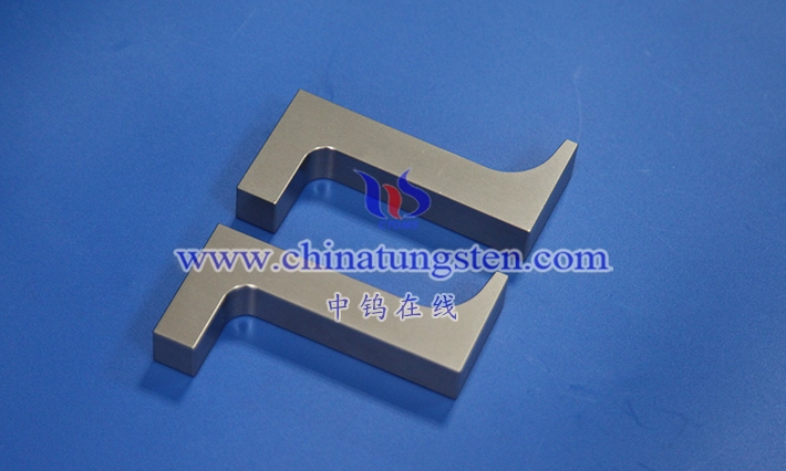
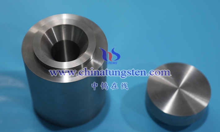
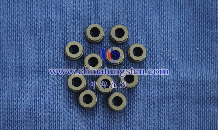
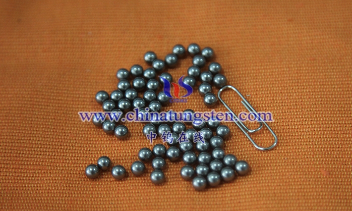
Chinatungsten Online and CTIA GROUP LTD provide products mainly including: tungsten oxide products, such as tungstates such as APT/WO3; tungsten powder and tungsten carbide powder; tungsten metal products such as tungsten wire, tungsten ball, tungsten bar, tungsten electrode, etc.; high-density alloy products, such as dart rods, fishing sinkers, automotive tungsten crankshaft counterweights, mobile phones, clocks and watches, tungsten alloy shielding materials for radioactive medical equipment, etc.; tungsten silver and tungsten copper products for electronic appliances. Cemented carbide products include cutting tools such as cutting, grinding, milling, drilling, planing, wear-resistant parts, nozzles, spheres, anti-skid spikes, molds, structural parts, seals, bearings, high-pressure and high-temperature resistant cavities, top hammers, and other standard and customized high-hardness, high-strength, strong acid and alkali resistant high-performance products. Molybdenum products include molybdenum oxide, molybdenum powder, molybdenum and alloy sintering materials, molybdenum crucibles, molybdenum boats, TZM, TZC, molybdenum wires, molybdenum heating belts, molybdenum spouts, molybdenum copper, molybdenum tungsten alloys, molybdenum sputtering targets, sapphire single crystal furnace components, etc.
For more information about tungsten carbide products, please visit the website: tungsten-carbide.com.cn
If you are interested in related products, please contact us:
Email: sales@chinatungsten.com
Tel: +86 592 5129696 / 86 592 5129595