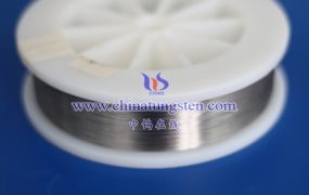
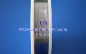
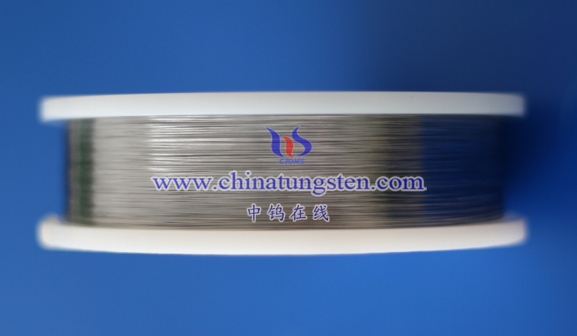
Cleaned tungsten wire plays a critical role in semiconductor manufacturing, primarily in the following processes:
- Heating Element: In chemical vapor deposition (CVD) or physical vapor deposition (PVD) equipment, cleaned tungsten wire serves as a heating source to heat substrates or evaporate materials, facilitating the growth of silicon-based films (such as silicon dioxide) or metal films (such as tungsten compounds). Its high temperature resistance and thermal stability ensure precise control of process temperatures.
- Electrode and Conductor: In ion implanters or plasma etching equipment, cleaned tungsten wire is used as an electrode or conductor. Its high electrical conductivity and corrosion resistance make it suitable for high-vacuum and strong electric field environments.
- Sputtering Target: Cleaned tungsten wire or tungsten-based materials can be processed into sputtering targets for depositing tungsten metal layers or tungsten compound layers (such as WSi₂), widely used in chip interconnects, gate electrodes, or barrier layers.
- Probe Material: In wafer testing, cleaned tungsten wire is used as a probe due to its high hardness and conductivity, allowing contact with chip pads to test circuit performance.
The high purity and stability of cleaned tungsten wire are essential for the cleanliness and reliability of semiconductor processes.
More details of tungsten wire, please visit website: http://www.tungsten-wire.com.cn/
Please contact CHINATUNGSTEN for inquiry and order of tungsten wire:
Email: sales@chinatungsten.com
Tel.: +86 592 5129595