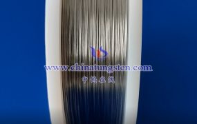
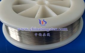
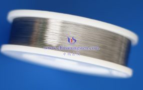
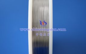
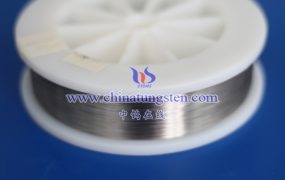
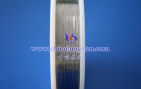
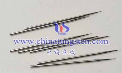
Tungsten probe for materials research usually refers to a detector used in the fields of materials science and engineering to characterize and study the properties of materials. These probes are usually made of tungsten to meet the specific needs and conditions in research.
Here are some possible applications and features of tungsten probes used in materials research:
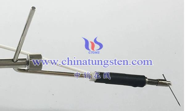
1. Atomic force microscopy (AFM): In AFM, tungsten probes can be used for surface topology imaging to obtain high-resolution information on the sample surface.
2. Electron Microscopy (EM): In electron microscopy, especially in high-resolution TEM (transmission electron microscopy), a tungsten probe may be used to generate a small electron beam for high-resolution sample imaging.
3. Scanning tunneling microscope (STM): In STM, a tungsten probe can be used to measure the electronic state of the sample surface and achieve atomic-level resolution.
4. Surface analysis and material characterization: Tungsten probes may be used in surface analysis instruments, such as mass spectrometers, surface plasma mass spectrometers (SIMS), etc., for material characterization and analysis.
5. Force spectroscopy: Tungsten probes may also have applications in the study of mechanical properties, such as measuring the elastic modulus of samples through atomic force microscopy (AFM).
More details of tungsten needles, please visit website: http://tungsten.com.cn/tungsten-needles-and-pins.html
Please contact CHINATUNGSTEN for inquiry and order of tungsten needles:
Email: sales@chinatungsten.com
Tel.: +86 592 5129595