Wafer test tungsten probe station is an instrument used for semiconductor wafer testing. It is mainly used to test the performance and reliability of integrated circuit devices on the wafer.
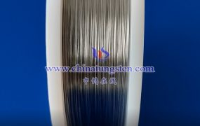
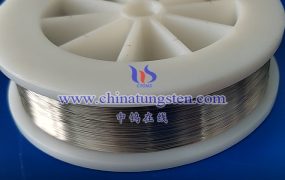
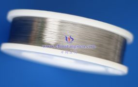
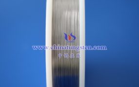
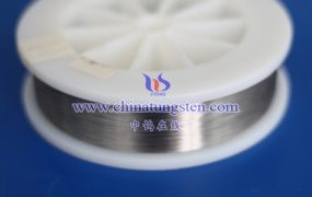
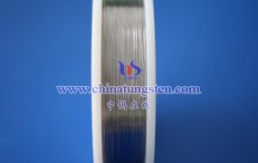
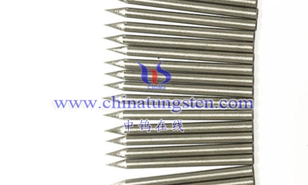
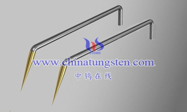
Wafer testing tungsten probe station usually consists of tungsten probe, positioner and control system. Tungsten probes are used to contact integrated circuit devices on wafers. They are usually made of high-purity tungsten, which has the advantages of high strength, high hardness and good corrosion resistance. The positioner is used to accurately move and position the tungsten probe. It usually consists of a precision mechanical system and a control system, which can achieve micron-level precision control of the tungsten probe. The control system is used to control parameters such as the movement trajectory and positioning accuracy of the tungsten probe. It is usually composed of a computer program or a controller.
Wafer testing tungsten probe station has a wide range of applications. For example, in the semiconductor industry, it is used for wafer-level processing and manufacturing; in the field of nanoscience research, it is used for atomic force microscopy and scanning tunneling microscopy. and other experiments; in the field of life sciences, it is used for cell manipulation, molecular biology experiments, etc.
The wafer testing tungsten probe station is a high-precision and high-reliability experimental equipment that can achieve precise control and measurement of integrated circuit devices on semiconductor wafers, providing important technical support for scientific research.
More details of tungsten needles, please visit website: http://tungsten.com.cn/tungsten-needles-and-pins.html
Please contact CHINATUNGSTEN for inquiry and order of tungsten needles:
Email: sales@chinatungsten.com
Tel.: +86 592 5129595