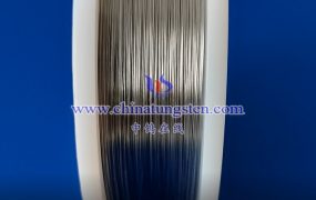
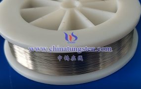
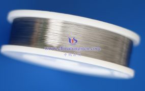
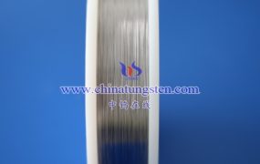
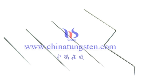
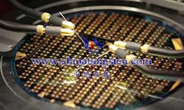
Wafer testing tungsten pin is a probe needle used for integrated circuit wafer testing, which is made of tungsten material. During wafer testing, this probe contacts each die on the chip to test its electrical properties. By using wafer testing tungsten pins, defects and issues on the chip can be detected, ensuring the quality and performance of each die meets requirements.
The manufacturing process of straight tungsten pins for wafer testing includes the following steps:
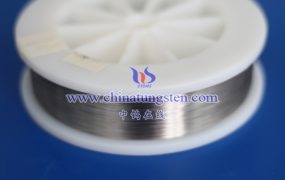
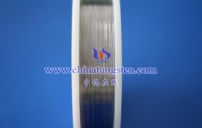
1. Material selection: Use high-purity tungsten material to ensure the stability and durability of the detection needle.
2. Probe manufacturing: Using precise micro-machining technology, the tungsten material is processed into an elongated probe shape. The diameter of the probe is usually in the micron range, and the length depends on the size of the wafer and the test needs.
3. Surface treatment: The surface of the probe is polished and gold-plated to improve the conductivity and corrosion resistance of the probe.
4. Installation and fixation: Install the probe on a stable base, and use springs and other mechanisms to buffer and fix the probe to ensure the stability and accuracy of the probe during the test.
More details of tungsten needles, please visit website: http://tungsten.com.cn/tungsten-needles-and-pins.html
Please contact CHINATUNGSTEN for inquiry and order of tungsten needles:
Email: sales@chinatungsten.com
Tel.: +86 592 5129595