Although wafer testing tungsten probes offer many advantages in semiconductor manufacturing, there are also some potential issues or challenges:
1. Cost: Tungsten is a high-cost material, and manufacturing and processing small-sized test probes may require specialized equipment and technology, which may result in relatively high manufacturing costs.
2. Brittleness: Despite its high hardness, tungsten is also relatively brittle. Under some extreme conditions, such as high temperatures or high pressures, tungsten probes may be more susceptible to mechanical stress and damage.
3. Thermal conductivity: Although tungsten has good electrical conductivity, its thermal conductivity is relatively low. This can become a problem in some test environments where cooling is required.
4. Wear: Since wafer testing is a highly repetitive process, test tungsten probes may experience wear. This can lead to changes in the geometry of the probe, which can affect the accuracy and consistency of the test.
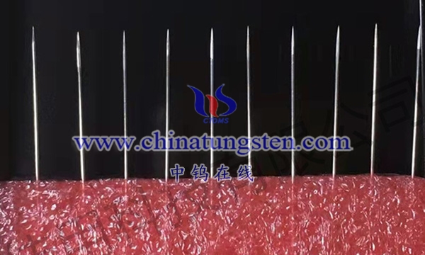
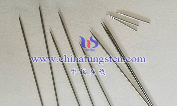
5. Micro size challenges: Manufacturing micro size test probes may face manufacturing process challenges. Maintaining probe accuracy and consistency can require highly sophisticated manufacturing techniques.
6. Adaptability issues: In some special testing environments, the adaptability of tungsten probes may be limited. For example, tungsten’s corrosion resistance can be an issue in some highly corrosive or chemically reactive environments.
These issues are often considerations during the design and manufacturing process, and manufacturers often work to resolve or mitigate them through improved materials and processes.
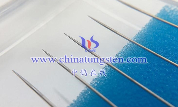
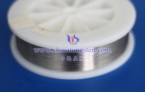
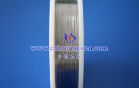
More details of tungsten needles, please visit website: http://tungsten.com.cn/tungsten-needles-and-pins.html
Please contact CHINATUNGSTEN for inquiry and order of tungsten needles:
Email: sales@chinatungsten.com
Tel.: +86 592 5129595