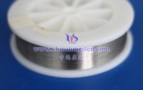
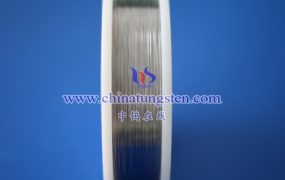
1. Providing high-energy electron beams: Tungsten wire probes can generate high-energy electron beams. These electron beams can excite various physical and chemical information of the sample when scanning the sample surface. For example, electron beams can be used to excite the electronic transition of the sample, thereby obtaining information such as the energy band structure of the sample.
2. Improve image resolution: Because the tungsten wire probe can generate high-energy electron beams, higher-resolution images can be obtained. This is important for studying materials and structures at the nanoscale.
3. Realize elemental analysis: By using a tungsten wire probe as the electron source, elemental analysis of the sample can also be realized. For example, the type and content of each element in the sample can be determined by performing energy dispersion spectroscopy (EDS) analysis on the sample surface.
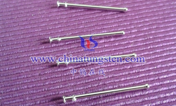
4. Enhance the conductivity of the sample: In some cases, the sample may accumulate charge during the electron beam scanning process due to charging effects, resulting in image distortion. By using a tungsten wire probe as the electron source, the conductivity of the sample can be enhanced, thereby reducing the impact of charging effects.
5. Achieve fast scanning: The electron beam generated by the tungsten wire probe has a higher current density, which allows the sample surface to be scanned faster, thus improving testing efficiency.
6. Adapt to a variety of test modes: The tungsten wire probe can adapt to a variety of test modes, such as bright field imaging, dark field imaging, micro-area component analysis, etc. This allows the same tungsten wire probe to be used for many different tests, increasing testing efficiency and convenience.
More details of tungsten probes, please visit website: http://tungsten.com.cn/tungsten-needles-and-pins.html
Please contact CHINATUNGSTEN for inquiry and order of tungsten needles:
Email: sales@chinatungsten.com
Tel.: +86 592 5129595
