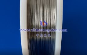
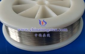
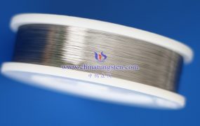
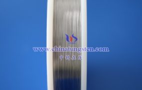
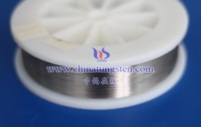
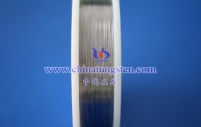
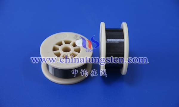
The tungsten wire used in photovoltaic crystalline silicon cutting is often called “silicon cutting wire” or “silicon wafer cutting wire”. It is a filament made of extremely pure tungsten material and is used to divide silicon wafers (also known as silicon wafers). wafers) to manufacture solar panels. These wafers are the basic building blocks of solar panels and are created by cutting blocks of silicon.
Here are some key features and applications of tungsten wire for photovoltaic crystalline silicon cutting:
High-temperature stability: The photovoltaic crystalline silicon cutting process needs to be carried out at extremely high temperatures, and tungsten has a very high melting point (approximately 3,422 degrees Celsius or 6,192 degrees Fahrenheit), so it remains stable in high-temperature environments and is not easy to melt or deform.
High Hardness: Tungsten is a very hard metal, making it suitable for applications such as cutting silicon wafers, which require high hardness. It can effectively cut silicon materials without wearing easily.
Filament Diameter: Cutting wires typically have very small diameters, typically between tens to hundreds of microns. This filament enables precise cutting of silicon wafers.
Corrosion Resistance: Tungsten is somewhat resistant to corrosion, which is critical when operating in silicon cutting fluids.
High strength: Tungsten wires generally have high strength, which allows them to remain stable and difficult to break when cutting silicon wafers.
More details of tungsten wire, please visit website: http://tungsten.com.cn/tungsten-wires.html
Please contact CHINATUNGSTEN for inquiry and order of tungsten wires.
Email: sales@chinatungsten.com
Tel.: +86 592 5129595