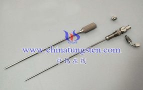
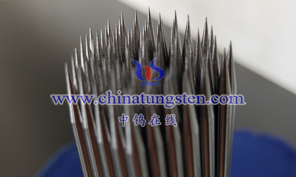
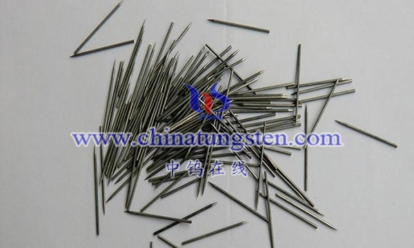
An electron microscope tungsten probe refers to a probe used in electron microscopes, the tip of which is mainly made of tungsten. An Electron Microscope (EM) is a microscope that uses a beam of electrons instead of light to magnify details in a sample. In electron microscopy, a tungsten probe is used as the electron emission source, which allows high-resolution and high-contrast images to be obtained.
Here are some features and applications of tungsten probes for electron microscopy:
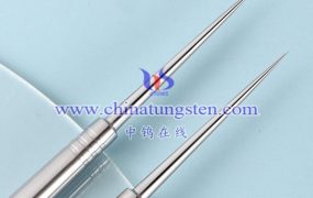
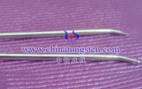
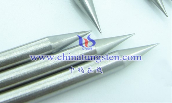
1. Tip shape: The tip of a tungsten probe is usually nanoscale and has a very sharp shape. This sharp tip helps produce a high-resolution electron beam.
2. High melting point: Tungsten has a high melting point (3422 degrees Celsius), so it is not easily melted under electron beam irradiation, helping to maintain the stability of the probe.
3. Electrical conductivity: Tungsten is an excellent conductive material that helps generate and maintain an electron beam at the probe tip.
4. High-resolution imaging: The electron microscope tungsten probe is used for high-resolution imaging, which can observe the structure and morphology of the sample at the nanometer scale.
5. Sample surface imaging: The electron microscope tungsten probe can be used for surface topology imaging to observe the surface morphology of the sample with high resolution.
This type of probe is widely used in a variety of scientific research and laboratory applications, including physics, biology, materials science, and more. It should be noted that the design and preparation of specific electron microscopy tungsten probes may vary to suit different experimental conditions and research purposes.
More details of tungsten needles, please visit website: http://tungsten.com.cn/tungsten-needles-and-pins.html
Please contact CHINATUNGSTEN for inquiry and order of tungsten needles:
Email: sales@chinatungsten.com
Tel.: +86 592 5129595