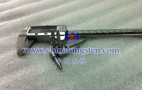
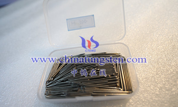
The scanning tunneling microscope (STM) tungsten probe is an electron detector used in STM with a tip made primarily of tungsten. STM is a surface science technology that uses the tunneling effect to detect the atomic and molecular structure of the sample surface. STM enables surface imaging and measurements at the atomic scale.
The following are some features and applications of STM tungsten probes:
1. Tip shape: The tip of the STM tungsten probe is very sharp, usually on the nanometer scale. This sharp tip helps create extremely small electron tunnels on the sample surface.
2. Electrical conductivity: Tungsten is an excellent conductive material and is therefore suitable for creating and maintaining electron tunnels at the probe tip.
3. High-resolution imaging: The STM tungsten probe can be used to achieve high-resolution surface imaging and can observe the topology and structure of the sample at the atomic scale.
4. Atomic resolution: Due to the utilization of the tunneling effect of electrons, STM can achieve atomic-level resolution, allowing scientists to observe and manipulate individual atoms.
5. Surface analysis: STM is widely used in the fields of surface science and materials science to study the surface structure, surface reaction and electronic properties of materials.
In STM, the current generated by electron tunneling is measured and recorded, which reflects the topology and electronic structure of the sample surface. STM is widely used in various scientific research and laboratory applications, providing a powerful tool for studying nanomaterials, surface catalysis, nanodevices, etc.

More details of tungsten needles, please visit website: http://tungsten.com.cn/tungsten-needles-and-pins.html
Please contact CHINATUNGSTEN for inquiry and order of tungsten needles:
Email: sales@chinatungsten.com
Tel.: +86 592 5129595