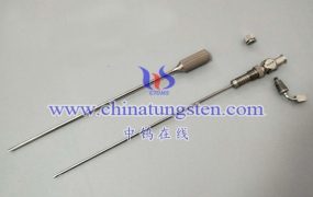
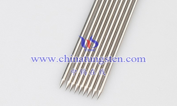
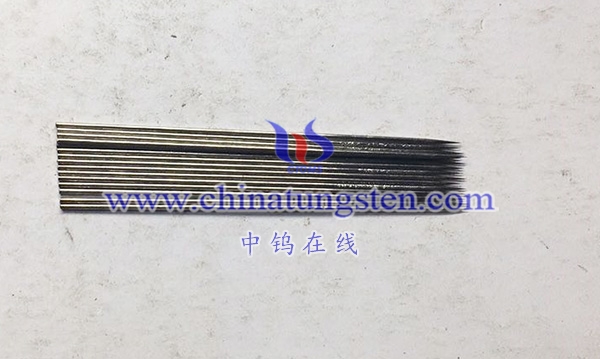
STM tungsten probe refers to the detector or electron probe used in scanning tunneling microscopy (STM), whose tip is mainly made of tungsten. STM is a high-resolution microscopy technique that uses the tunneling effect of electrons to measure and image the atomic structure of a sample surface.
The following are some features and applications of STM tungsten probes:
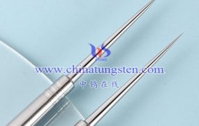
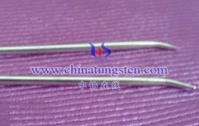
1. Tip shape: The tip of an STM tungsten probe is usually very sharp, with dimensions at the nanometer level. This sharp tip helps form tiny electron tunnels on the sample surface.
2. Electrical conductivity: Tungsten is a good conductive material and is suitable for creating and maintaining electron tunnels at the probe tip.
3. High-resolution imaging: The STM tungsten probe can be used for high-resolution surface imaging and can observe the topology and structure of the sample at the atomic scale.
4. Atomic resolution: Using the tunneling effect of electrons, STM can achieve atomic-level resolution, allowing scientists to observe and manipulate individual atoms.
5. Surface analysis: STM is widely used in the fields of surface science and materials science to study the surface structure, surface reaction and electronic properties of materials.
In STM, the STM tungsten probe obtains information about the sample surface by measuring the tunneling current of electrons. This technique is very useful and can be used to study nanostructures, surface catalysis, nanodevices, etc. Due to its high resolution and atomic-level sensitivity, STM has become a key tool in surface science and nanotechnology research.
 ‘
‘
More details of tungsten needles, please visit website: http://tungsten.com.cn/tungsten-needles-and-pins.html
Please contact CHINATUNGSTEN for inquiry and order of tungsten needles:
Email: sales@chinatungsten.com
Tel.: +86 592 5129595